DLPU101D December 2020 – July 2024 DLPC900
- 1
- Trademarks
- Read This First
- 1 About This Guide
- 2 Related Documentation from Texas Instruments
- 3 If You Need Assistance
- 4 DLP LightCrafter Single DLPC900 EVM Overview
- 5 Quick Start
-
6 Operating the
DLP LightCrafter Single DLPC900 EVM
- 6.1 DLP LightCrafter Single DLPC900 Control Software
- 6.2 PC Software
- 6.3 System Common Controls
- 6.4 System Settings
- 6.5 Video Mode
- 6.6
Pattern Modes
- 6.6.1 Menu Bar
- 6.6.2 Creating a Pattern Sequence in Pattern On-The-Fly Mode
- 6.6.3 Creating a Pattern Sequence in Pre-Stored Pattern Mode
- 6.6.4 Reordering a Pattern Sequence using the Edit LUT Feature
- 6.6.5 Creating a Pattern Sequence in Video Pattern Mode
- 6.6.6 Creating a Pattern Sequence With DMD Block Load
- 6.6.7 Pattern Settings
- 6.7 Batch Files
- 6.8 Peripherals
- 6.9 Firmware
- 6.10 Flash Device Parameters
- 6.11 JTAG Flash Programming
- 6.12 Programming an EDID
- 7 Connectors
- 8 Power Supply Requirements
- 9 Safety
- 10Revision History
4.5 DLP LightCrafter Single DLPC900 Connections
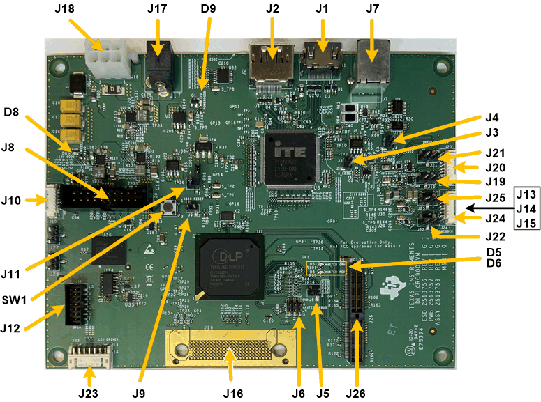
Figure 4-3 depicts the switches and connectors with the respective locations.
Note: Power supply (and cable), USB cable, and display cable are
NOT included with the module.
 Figure 4-3 DLP
LightCrafter Single DLPC900 EVM Connectors (Top View)
Figure 4-3 DLP
LightCrafter Single DLPC900 EVM Connectors (Top View)Table 4-1 DLP LightCrafter Single
DLPC900 EVM Connector Reference
| Connector Reference | EVM Function | Description or Use |
|---|---|---|
| SW1 | Hardware Reset Switch | When pressed resets the DLPC900 controller. When released, the controller boots from reset. |
| J1 | HDMI Input | HDMI video input (primary). |
| J2 | DisplayPort Input | DisplayPort video input (secondary). |
| J3 | EDID jumper (HDMI) | When jumper is installed, the EDID prom for the HDMI interface can be updated. |
| J4 | EDID jumper (DisplayPort) | When jumper is installed, the EDID prom for the DisplayPort interface can be updated. |
| J5 | OCLKA output | User configurable DLPC900 output clock for additional user on board logic. Pin 1 = OCLKA; Pin 2 = GND |
| J6 | DLPC900 debug UART | DLPC900 UART interface for debug messages to a
terminal
|
| J7 | Host USB interface | DLPC900 USB interface for Host communications with DLPC900 |
| J8 | ARM RVI ICE debugger | TI use only; Used for debugging DLPC900 ARM software code, requires the ARM RVI ICE debugger. |
| J9 | DLPC900 Reset jumper | When jumper is installed, the controller is held in RESET. |
| J10 | JTAG Boundary Scan | Used for programming the boot image into the flash memory when flash memory is blank or corrupted. |
| J11 | BOOTHold jumper | When jumper is installed, forces the controller to remain in boot mode when power is applied. |
| J12 | GPIO inputs/outputs | User configurable general purpose Inputs and/or outputs for customer use. |
| J13 | Host I2C Port 0 | Host dedicated I2C interface port for communications to DLPC900. [Pin 1 = SCL, Pin 2 = SDA, Pin 3 = 3.3V, Pin 4 = GND] |
| J14 | Host I2C Port 1 | I2C interface port for programming EDID UARTs via I2C [ Pin 1 = SCL, Pin 2 = SDA, Pin 3 = 3.3V, Pin 4 = GND] |
| J15 | Host I2C Port 2 | I2C interface port 2. For TI internal use. [ Pin 1 = SCL, Pin 2 = SDA, Pin 3 = 3.3V, Pin 4 = GND] |
|
Note:
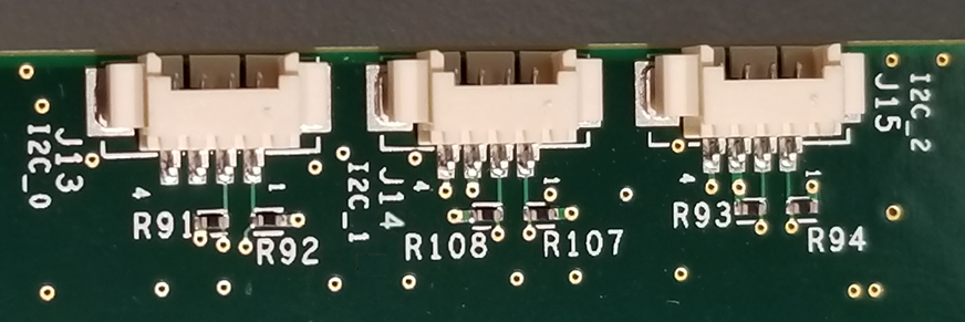
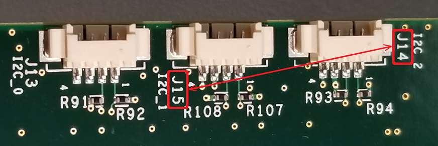
On several board lots, the silk screen jumper labels J14 and J15 are swapped. Labels I2C_1 and I2C_2 on all boards are correct. The correct jumper labels are I2C_1 is J14 and I2C_2 is J15.  Figure 4-4 Correct
J14 and J15 Labels
 Figure 4-5 Incorrect
J14 and J15 Labels
 |
||
| J16 | DMD flex connector (DLPC900) | Flex cable connection for data interface to DMD board and DMD. |
| J17 | +12 VDC Power input | EVM power input. [Pin 1 = +12 VDC, Pin 2,3 = GND] See Section 8.1. |
| J18 | +12 VDC Power input (Alternate) | EVM power alternate input. [Pin 1,2,3 = GND, Pin 4,5,6 = +12 VDC] See Section 8.1. |
| J19 | Trigger Input 1 voltage level selectors. | Set the voltage levels of the Trigger Input 1
signals.
|
| J20 | External Input Triggers connector | Trigger input 1 and 2 for triggering the DLPC900 with external input signals (from cameras, processors). See Section 7.1. |
| J21 | Trigger Input 2 voltage level selectors. | Set the voltage levels of the trigger input 2
signals.
|
| J22 | Trigger Output 1 voltage level selectors | Set the voltage levels of the trigger output 1
signals.
|
| J23 | LED illuminator enables and PWM drive signals |
|
| J24 | Trigger Output connector | Trigger outputs 1 and 2 for triggering external devices. See Section 7.2. |
| J25 | Trigger Output 2 voltage level selectors | Set the voltage levels of the Trigger Output 2
signals.
|
| J26 | External Parallel Video Connector | Used for direct connection to an external parallel video source. |
| D5 | DLPC900 Red fault status LED | When lit indicates a fault has occurred in the DLPC900 controller. |
| D6 | DLPC900 Green Heartbeat LED | When toggling indicates DLPC900 controller is
operating. Note: The heartbeat operates even if no DMD is
present. |
| D8 | 12V Power LED | When lit indicates external 12V supply is on. |
| D9 | PWRGOOD LED | When lit indicates power is within the expected limits. |