JAJS365D January 2007 – October 2019 TPS2412 , TPS2413
PRODUCTION DATA.
- 1 特長
- 2 アプリケーション
- 3 概要
- 4 改訂履歴
- 5 概要(続き)
- 6 Device Comparison Table
- 7 Pin Configuration and Functions
- 8 Specifications
-
9 Detailed Description
- 9.1 Overview
- 9.2 Functional Block Diagram
- 9.3
Feature Description
- 9.3.1 Definitions
- 9.3.2 TPS2412 vs TPS2413 – MOSFET Control Methods
- 9.3.3 N+1 Power Supply – Typical Connection
- 9.3.4 Input ORing – Typical Connection
- 9.3.5 System Design and Behavior With Transients
- 9.3.6 TPS2412 Regulation-Loop Stability
- 9.3.7 MOSFET Selection and R(RSET)
- 9.3.8 Gate Drive, Charge Pump and C(BYP)
- 9.4 Device Functional Modes
- 10Application and Implementation
- 11Power Supply Recommendations
- 12Layout
- 13デバイスおよびドキュメントのサポート
- 14メカニカル、パッケージ、および注文情報
9.3.3 N+1 Power Supply – Typical Connection
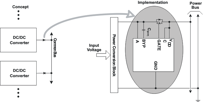
The N+1 power supply configuration shown in Figure 9 is used where multiple power supplies are paralleled for either higher capacity, redundancy or both. If it takes N supplies to power the load, adding an extra, identical unit in parallel permits the load to continue operation in the event that any one of the N supplies fails. The supplies are ORed together, rather than directly connected to the bus, to isolate the converter output from the bus when it is plugged-in or fails short. The TPS2412/13 with an external MOSFET emulates the function of the ORing diode.
It is possible for a malfunctioning converter in an ORed topology to create a bus overvoltage if the loading is less than the converter's capacity (for example, N = 1). The ORed topology shown cannot protect the bus from this condition, even if the ORing MOSFET can be turned off. One common solution is to use two MOSFETs in a back-to-back configuration to provide bidirectional blocking. The TPS2412/13 does not have a provision for forcing the gate off when the overvoltage condition occurs, use of the TPS2410/11 is recommended.
ORed supplies are usually designed to share power by various means, although the desired operation could implement an active and standby concept. Sharing approaches include both passive, or voltage droop, and active methods. Not all of the output ORing devices may be ON depending on the sharing control method, bus loading, distribution resistances, and TPS2412/13 settings.
 Figure 9. N+1 Power Supply Example