JAJS485F July 2009 – April 2017 TPA3110D2
PRODUCTION DATA.
- 1 特長
- 2 アプリケーション
- 3 概要
- 4 改訂履歴
- 5 Device Comparison Table
- 6 Pin Configuration and F unctions
- 7 Specifications
- 8 Parameter Measurement Information
-
9 Detailed Description
- 9.1 Overview
- 9.2 Functional Block Diagram
- 9.3 Feature Description
- 9.4 Device Functional Modes
- 10Application and Implementation
- 11Power Supply Recommendations
- 12Layout
- 13デバイスおよびドキュメントのサポート
- 14メカニカル、パッケージ、および注文情報
9 Detailed Description
9.1 Overview
The TPA3110D2 is a 15-W Class-D audio power amplifier. It is designed to drive BTL stereo speakers. This device is able to use inexpensive ferrite bead filters at the outputs while meeting EMC requirements. The TPA3110D2 can drive stereo speakers as low as 4 Ω and its high efficiency eliminates the need for an external heat sink. The device is fully protected against shorts to GND, VCC and output-to-output. The short-circuit protection and thermal protection includes an auto-recovery feature.
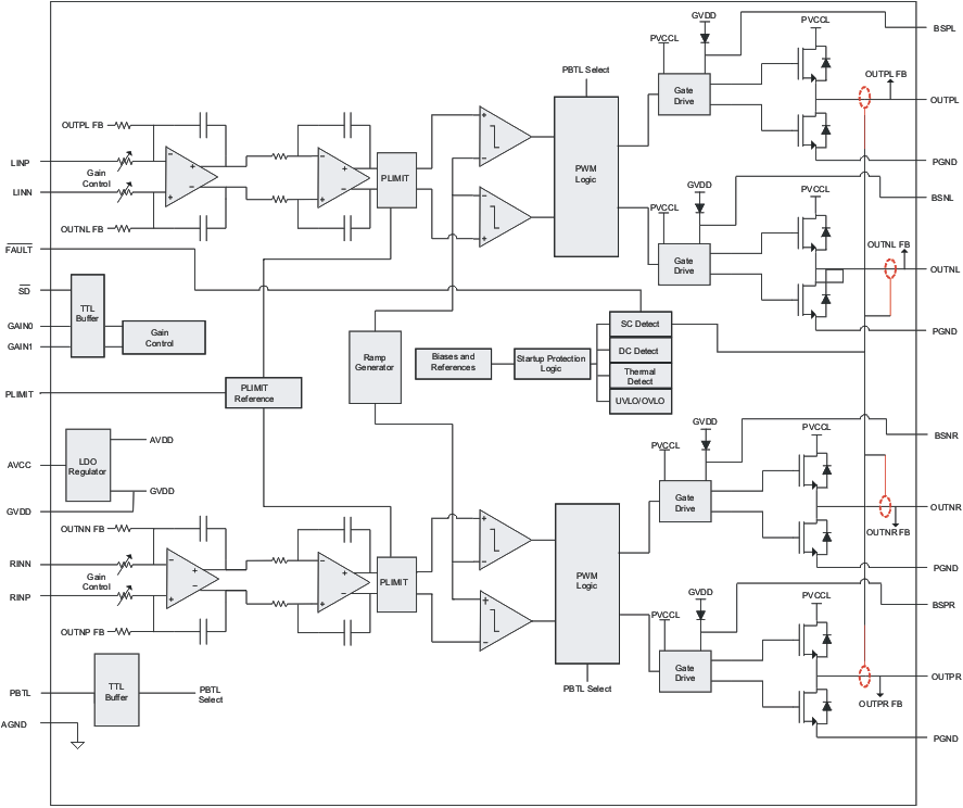
9.2 Functional Block Diagram
9.3 Feature Description
9.3.1 TPA3110D2 Modulation Scheme
The TPA3110D2 uses a modulation scheme that allows operation without the classic LC reconstruction filter when the amp is driving an inductive load. Each output is switching from 0 volts to the supply voltage. The OUTP and OUTN are in phase with each other with no input so that there is little or no current in the speaker. The duty cycle of OUTP is greater than 50% and OUTN is less than 50% for positive output voltages. The duty cycle of OUTP is less than 50% and OUTN is greater than 50% for negative output voltages. The voltage across the load sits at 0V throughout most of the switching period, reducing the switching current, which reduces any I2R losses in the load.
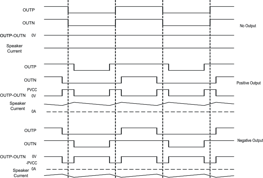 Figure 36. The TPA3110D2 Output Voltage And Current Waveforms Into An Inductive Load
9.3.1.1 Ferrite Bead Filter Considerations
Using the Advanced Emissions Suppression Technology in the TPA3110D2 amplifier it is possible to design a high efficiency Class-D audio amplifier while minimizing interference to surrounding circuits. It is also possible to accomplish this with only a low-cost ferrite bead filter. In this case it is necessary to carefully select the ferrite bead used in the filter.
One important aspect of the ferrite bead selection is the type of material used in the ferrite bead. Not all ferrite material is alike, so it is important to select a material that is effective in the 10 to 100 MHz range which is key to the operation of the Class D amplifier. Many of the specifications regulating consumer electronics have emissions limits as low as 30 MHz. It is important to use the ferrite bead filter to block radiation in the 30 MHz and above range from appearing on the speaker wires and the power supply lines which are good antennas for these signals. The impedance of the ferrite bead can be used along with a small capacitor with a value in the range of 1000 pF to reduce the frequency spectrum of the signal to an acceptable level. For best performance, the resonant frequency of the ferrite bead/ capacitor filter should be less than 10 MHz.
Also, it is important that the ferrite bead is large enough to maintain its impedance at the peak currents expected for the amplifier. Some ferrite bead manufacturers specify the bead impedance at a variety of current levels. In this case it is possible to make sure the ferrite bead maintains an adequate amount of impedance at the peak current the amplifier will see. If these specifications are not available, it is also possible to estimate the bead current handling capability by measuring the resonant frequency of the filter output at low power and at maximum power. A change of resonant frequency of less than fifty percent under this condition is desirable. Examples of ferrite beads which have been tested and work well with the TPA3110D2 include 28L0138-80R-10 and HI1812V101R-10 from Steward and the 742792510 from Wurth Electronics.
A high quality ceramic capacitor is also needed for the ferrite bead filter. A low ESR capacitor with good temperature and voltage characteristics will work best.
Additional EMC improvements may be obtained by adding snubber networks from each of the class D outputs to ground. Suggested values for a simple RC series snubber network would be 10 Ω in series with a 330 pF capacitor although design of the snubber network is specific to every application and must be designed taking into account the parasitic reactance of the printed circuit board as well as the audio amp. Take care to evaluate the stress on the component in the snubber network especially if the amp is running at high PVCC. Also, make sure the layout of the snubber network is tight and returns directly to the PGND or the PowerPAD™ beneath the chip.
 Figure 37. TPA3110D2 EMC Spectrum With FCC Class B Limits
9.3.1.2 Efficiency: LC Filter Required With The Traditional Class-D Modulation Scheme
The main reason that the traditional class-D amplifier needs an output filter is that the switching waveform results in maximum current flow. This causes more loss in the load, which causes lower efficiency. The ripple current is large for the traditional modulation scheme, because the ripple current is proportional to voltage multiplied by the time at that voltage. The differential voltage swing is 2 × VCC, and the time at each voltage is half the period for the traditional modulation scheme. An ideal LC filter is needed to store the ripple current from each half cycle for the next half cycle, while any resistance causes power dissipation. The speaker is both resistive and reactive, whereas an LC filter is almost purely reactive.
The TPA3110D2 modulation scheme has little loss in the load without a filter because the pulses are short and the change in voltage is VCC instead of 2 × VCC. As the output power increases, the pulses widen, making the ripple current larger. Ripple current could be filtered with an LC filter for increased efficiency, but for most applications the filter is not needed.
An LC filter with a cutoff frequency less than the class-D switching frequency allows the switching current to flow through the filter instead of the load. The filter has less resistance but higher impedance at the switching frequency than the speaker, which results in less power dissipation, therefore increasing efficiency.
9.3.1.3 When to Use an Output Filter for EMI Suppression
The TPA3110D2 has been tested with a simple ferrite bead filter for a variety of applications including long speaker wires up to 125 cm and high power. The TPA3110D2 EVM passes FCC Class B specifications under these conditions using twisted speaker wires. The size and type of ferrite bead can be selected to meet application requirements. Also, the filter capacitor can be increased if necessary with some impact on efficiency.
There may be a few circuit instances where it is necessary to add a complete LC reconstruction filter. These circumstances might occur if there are nearby circuits which are sensitive to noise. In these cases a classic second order Butterworth filter similar to those shown in the figures below can be used.
Some systems have little power supply decoupling from the AC line but are also subject to line conducted interference (LCI) regulations. These include systems powered by "wall warts" and "power bricks." In these cases, it LC reconstruction filters can be the lowest cost means to pass LCI tests. Common mode chokes using low frequency ferrite material can also be effective at preventing line conducted interference.
 Figure 38. Typical LC Output Filter, Cutoff Frequency of 27 Khz, Speaker Impedance = 8 Ω
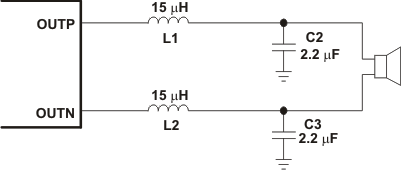 Figure 39. Typical Lc Output Filter, Cutoff Frequency Of 27 Khz, Speaker Impedance = 4 Ω
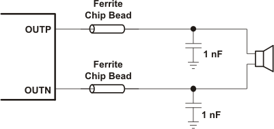 Figure 40. Typical Ferrite Chip Bead Filter (Chip Bead Example)
9.3.2 Gain Setting Via GAIN0 And GAIN1 Inputs
The gain of the TPA3110D2 is set by two input terminals, GAIN0 and GAIN1. The voltage slew rate of these gain terminals, along with terminals 1 and 14, must be restricted to no more than 10V/ms. For higher slew rates, use a 100kΩ resistor in series with the terminals.
The gains listed in Table 2 are realized by changing the taps on the input resistors and feedback resistors inside the amplifier. This causes the input impedance (ZI) to be dependent on the gain setting. The actual gain settings are controlled by ratios of resistors, so the gain variation from part-to-part is small. However, the input impedance from part-to-part at the same gain may shift by ±20% due to shifts in the actual resistance of the input resistors.
For design purposes, the input network (discussed in the next section) should be designed assuming an input impedance of 7.2 kΩ, which is the absolute minimum input impedance of the TPA3110D2. At the lower gain settings, the input impedance could increase as high as 72 kΩ
Table 2. Gain Setting
| GAIN1 | GAIN0 | AMPLIFIER GAIN (dB) | INPUT IMPEDANCE (kΩ) |
| TYP | TYP | ||
| 0 | 0 | 20 | 60 |
| 0 | 1 | 26 | 30 |
| 1 | 0 | 32 | 15 |
| 1 | 1 | 36 | 9 |
9.3.3 Differential Inputs
The differential input stage of the amplifier cancels any noise that appears on both input lines of the channel. To use the TPA3110D2 with a differential source, connect the positive lead of the audio source to the INP input and the negative lead from the audio source to the INN input. To use the TPA3110D2 with a single-ended source, ac ground the INP or INN input through a capacitor equal in value to the input capacitor on INN or INP and apply the audio source to either input. In a single-ended input application, the unused input should be ac grounded at the audio source instead of at the device input for best noise performance. For good transient performance, the impedance seen at each of the two differential inputs should be the same.
The impedance seen at the inputs should be limited to an RC time constant of 1 ms or less if possible. This is to allow the input dc blocking capacitors to become completely charged during the 14 ms power-up time. If the input capacitors are not allowed to completely charge, there will be some additional sensitivity to component matching which can result in pop if the input components are not well matched.
9.3.4 PLIMIT
The voltage at pin 10 can used to limit the power to levels below that which is possible based on the supply rail. Add a resistor divider from GVDD to ground to set the voltage at the PLIMIT pin. An external reference may also be used if tighter tolerance is required. Also add a 1μF capacitor from pin 10 to ground.
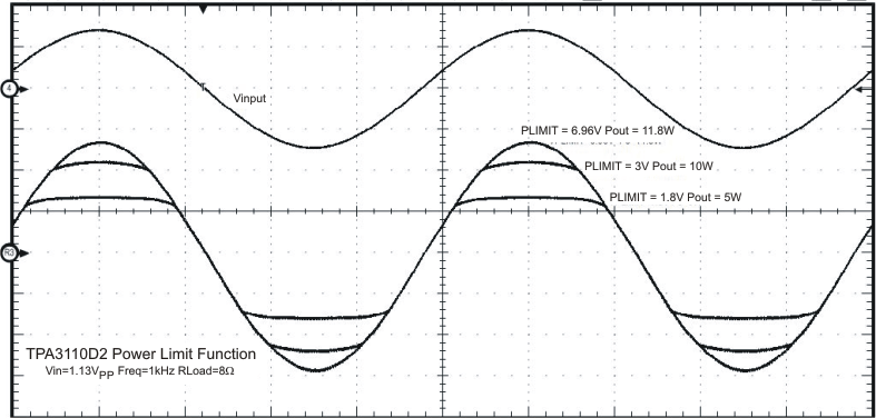 Figure 41. PLIMIT Circuit Operation
The PLIMIT circuit sets a limit on the output peak-to-peak voltage. The limiting is done by limiting the duty cycle to fixed maximum value. This limit can be thought of as a virtual voltage rail which is lower than the supply connected to PVCC. This "virtual" rail is 4 times the voltage at the PLIMIT pin. This output voltage can be used to calculate the maximum output power for a given maximum input voltage and speaker impedance.

where
- RS is the total series resistance including RDS(on), and any resistance in the output filter.
- RL is the load resistance.
- VP is the peak amplitude of the output possible within the supply rail.
- POUT (10%THD) = 1.25 × POUT (unclipped)
Table 3. PLIMIT Typical Operation
| TEST CONDITIONS | PLIMIT VOLTAGE | OUTPUT POWER (W) | OUTPUT VOLTAGE AMPLITUDE (VP-P) |
|---|---|---|---|
| PVCC=24V, Vin=1Vrms, RL=8Ω, Gain=26dB | 6.97 | 36.1 (thermally limited) | 43 |
| PVCC=24V, Vin=1Vrms, RL=8Ω, Gain=26dB | 2.94 | 15 | 25.2 |
| PVCC=24V, Vin=1Vrms, RL=8Ω, Gain=26dB | 2.34 | 10 | 20 |
| PVCC=24V, Vin=1Vrms, RL=8Ω, Gain=26dB | 1.62 | 5 | 14 |
| PVCC=24V, Vin=1Vrms, RL=8Ω, Gain=20dB | 6.97 | 12.1 | 27.7 |
| PVCC=24V, Vin=1Vrms, RL=8Ω, Gain=20dB | 3.00 | 10 | 23 |
| PVCC=24V, Vin=1Vrms, RL=8Ω, Gain=20dB | 1.86 | 5 | 14.8 |
| PVCC=12V, Vin=1Vrms, RL=8Ω, Gain=20dB | 6.97 | 10.55 | 23.5 |
| PVCC=12V, Vin=1Vrms, RL=8Ω, Gain=20dB | 1.76 | 5 | 15 |
9.3.5 GVDD Supply
The GVDD Supply is used to power the gates of the output full bridge transistors. It can also be used to supply the PLIMIT voltage divider circuit. Add a 1-μF capacitor to ground at this pin.
9.3.6 PBTL Select
TPA3110D2 offers the feature of parallel BTL operation with two outputs of each channel connected directly. If the PBTL pin (pin 14) is tied high, the positive and negative outputs of each channel (left and right) are synchronized and in phase. To operate in this PBTL (mono) mode, apply the input signal to the RIGHT input and place the speaker between the LEFT and RIGHT outputs. Connect the positive and negative output together for best efficiency. The voltage slew rate of the PBTL pin must be restricted to no more than 10V/ms. For higher slew rates, use a 100kΩ resistor in series with the terminals. For an example of the PBTL connection, see the schematic in the APPLICATION INFORMATION section.
For normal BTL operation, connect the PBTL pin to local ground.
9.3.7 Thermal Protection
Thermal protection on the TPA3110D2 prevents damage to the device when the internal die temperature exceeds 150°C. There is a ±15°C tolerance on this trip point from device to device. Once the die temperature exceeds the thermal set point, the device enters into the shutdown state and the outputs are disabled. This is not a latched fault. The thermal fault is cleared once the temperature of the die is reduced by 15°C. The device begins normal operation at this point with no external system interaction.
Thermal protection faults are NOT reported on the FAULT terminal.
9.3.8 DC Detect
TPA3110D2 has circuitry which will protect the speakers from DC current which might occur due to defective capacitors on the input or shorts on the printed circuit board at the inputs. A DC detect fault will be reported on the FAULT pin as a low state. The DC Detect fault will also cause the amplifier to shutdown by changing the state of the outputs to Hi-Z. To clear the DC Detect it is necessary to cycle the PVCC supply. Cycling S D will NOT clear a DC detect fault.
A DC Detect Fault is issued when the output differential duty-cycle of either channel exceeds 14% (for example, +57%, -43%) for more than 420 msec at the same polarity. This feature protects the speaker from large DC currents or AC currents less than 2Hz. To avoid nuisance faults due to the DC detect circuit, hold the SD pin low at power-up until the signals at the inputs are stable. Also, take care to match the impedance seen at the positive and negative inputs to avoid nuisance DC detect faults.
The minimum differential input voltages required to trigger the DC detect are show in table 2. The inputs must remain at or above the voltage listed in the table for more than 420 msec to trigger the DC detect.
Table 4. DC Detect Threshold
| AV(dB) | Vin (mV, differential) |
|---|---|
| 20 | 112 |
| 26 | 56 |
| 32 | 28 |
| 36 | 17 |
9.3.9 Short-Circuit Protection and Automatic Recovery Feature
TPA3110D2 has protection from overcurrent conditions caused by a short circuit on the output stage. The short circuit protection fault is reported on the FAULT pin as a low state. The amplifier outputs are switched to a Hi-Z state when the short circuit protection latch is engaged. The latch can be cleared by cycling the SD pin through the low state.
If automatic recovery from the short circuit protection latch is desired, connect the FAULT pin directly to the SD pin. This allows the FAULT pin function to automatically drive the SD pin low which clears the short-circuit protection latch.
9.4 Device Functional Modes
9.4.1 SD Operation
The TPA3110D2 employs a shutdown mode of operation designed to reduce supply current (ICC) to the absolute minimum level during periods of nonuse for power conservation. The SD input terminal should be held high (see specification table for trip point) during normal operation when the amplifier is in use. Pulling SD low causes the outputs to mute and the amplifier to enter a low-current state. Never leave SD unconnected, because amplifier operation would be unpredictable.
For the best power-off pop performance, place the amplifier in the shutdown mode prior to removing the power supply voltage.