JAJSAC1H November 2007 – October 2024 LM3481
PRODUCTION DATA
- 1
- 1 特長
- 2 アプリケーション
- 3 概要
- 4 Pin Configuration and Functions
- 5 Specifications
- 6 Detailed Description
-
7 Application and Implementation
- 7.1 Application Information
- 7.2
Typical Applications
- 7.2.1
Boost Converter
- 7.2.1.1 Design Requirements
- 7.2.1.2
Detailed Design Procedure
- 7.2.1.2.1 Custom Design with WEBENCH Tools
- 7.2.1.2.2 Power Inductor Selection
- 7.2.1.2.3 Programming the Output Voltage and Output Current
- 7.2.1.2.4 Current Limit With Additional Slope Compensation
- 7.2.1.2.5 Power Diode Selection
- 7.2.1.2.6 Power MOSFET Selection
- 7.2.1.2.7 Input Capacitor Selection
- 7.2.1.2.8 Output Capacitor Selection
- 7.2.1.2.9 Driver Supply Capacitor Selection
- 7.2.1.2.10 Compensation
- 7.2.1.3 Application Curve
- 7.2.2 Typical SEPIC Converter
- 7.2.1
Boost Converter
- 7.3 Power Supply Recommendations
- 7.4 Layout
- 8 Device and Documentation Support
- 9 Revision History
- 10Mechanical, Packaging, and Orderable Information
7.2.1 Boost Converter
 Figure 7-1 Typical High Efficiency Step-Up (Boost) Converter using LM3481
The most common topology for the LM3481 is the boost or step-up topology. The boost converter converts a low input voltage into a higher output voltage. The basic configuration for a boost regulator is shown in Figure 7-2. In continuous conduction mode (when the inductor current never reaches zero at steady state), the boost regulator operates in two cycles. In the first cycle of operation, MOSFET Q is turned on and energy is stored in the inductor. During this cycle, diode D1 is reverse biased and load current is supplied by the output capacitor, COUT.
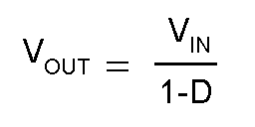
In the second cycle, MOSFET Q is off and the diode is forward biased. The energy stored in the inductor is transferred to the load and output capacitor. The ratio of these two cycles determines the output voltage. The output voltage is defined as:

(ignoring the voltage drop across the MOSFET and the diode), or

where D is the duty cycle of the switch, VD1 is the forward voltage drop of the diode, and VQ is the drop across the MOSFET when it is on. The following sections describe selection of components for a boost converter.
