JAJSBR5H
February 2012 – June 2018
TLV62130
,
TLV62130A
PRODUCTION DATA.
1
特長
2
アプリケーション
3
概要
Device Images
代表的なアプリケーションの回路図
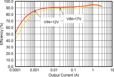
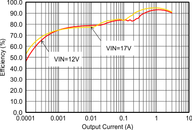
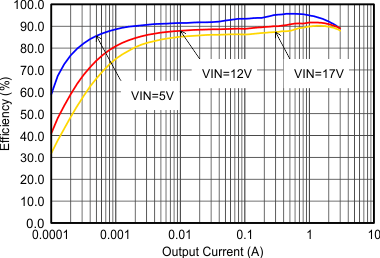
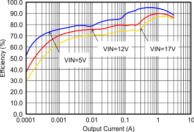
効率と出力電流との関係
4
改訂履歴
5
Device Comparison Table
6
Pin Configuration and Functions
Pin Functions
7
Specifications
7.1
Absolute Maximum Ratings
7.2
ESD Ratings
7.3
Recommended Operating Conditions
7.4
Thermal Information
7.5
Electrical Characteristics
7.6
Typical Characteristics
8
Detailed Description
8.1
Overview
8.2
Functional Block Diagram
8.3
Feature Description
8.3.1
Enable / Shutdown (EN)
8.3.2
Soft Start / Tracking (SS/TR)
8.3.3
Power Good (PG)
8.3.4
Pin-Selectable Output Voltage (DEF)
8.3.5
Frequency Selection (FSW)
8.3.6
Undervoltage Lockout (UVLO)
8.3.7
Thermal Shutdown
8.4
Device Functional Modes
8.4.1
Pulse Width Modulation (PWM) Operation
8.4.2
Power Save Mode Operation
8.4.3
100% Duty-Cycle Operation
8.4.4
Current Limit and Short Circuit Protection
9
Application and Implementation
9.1
Application Information
9.2
Typical Application
9.2.1
Design Requirements
9.2.2
Detailed Design Procedure
9.2.2.1
Custom Design With WEBENCH® Tools
9.2.2.2
Programming the Output Voltage
9.2.2.3
External Component Selection
9.2.2.3.1
Inductor Selection
9.2.2.3.2
Capacitor Selection
9.2.2.3.2.1
Output Capacitor
9.2.2.3.2.2
Input Capacitor
9.2.2.3.2.3
Soft Start Capacitor
9.2.2.4
Tracking Function
9.2.2.5
Output Filter and Loop Stability
9.2.3
Application Curves
9.3
System Examples
9.3.1
LED Power Supply
9.3.2
Active Output Discharge
9.3.3
Inverting Power Supply
9.3.4
Various Output Voltages
10
Power Supply Recommendations
11
Layout
11.1
Layout Guidelines
11.2
Layout Example
11.3
Thermal Considerations
12
デバイスおよびドキュメントのサポート
12.1
デバイス・サポート
12.1.1
デベロッパー・ネットワークの製品に関する免責事項
12.1.2
開発サポート
12.1.2.1
WEBENCH®ツールによるカスタム設計
12.2
ドキュメントの更新通知を受け取る方法
12.3
ドキュメントのサポート
12.3.1
関連資料
12.4
関連リンク
12.5
コミュニティ・リソース
12.6
商標
12.7
静電気放電に関する注意事項
12.8
Glossary
13
メカニカル、パッケージ、および注文情報
9.2.3
Application Curves
V
IN
= 12 V, V
OUT
= 3.3 V, T
A
= 25°C, (unless otherwise noted)
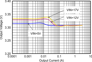
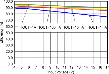
Figure 8.
Efficiency With 1.25 MHz, Vout = 5 V
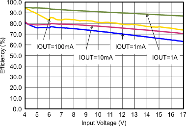
Figure 10.
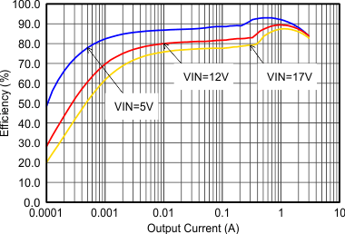
Efficiency With 2.5 MHz, Vout = 5 V
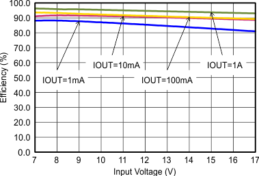
Figure 12.
Efficiency With 1.25 MHz, Vout = 3.3 V
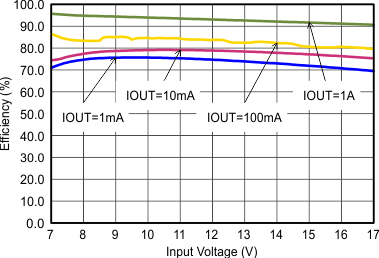
Figure 14.
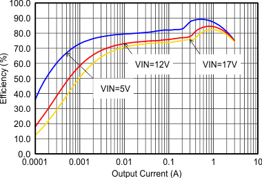
Efficiency With 2.5 MHz, Vout = 3.3 V
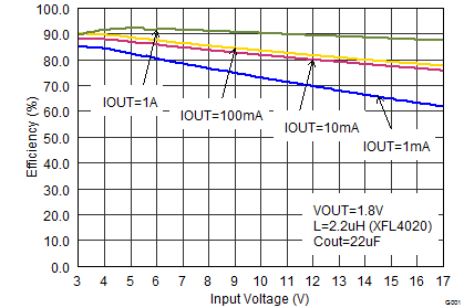
Figure 16.
Efficiency With 1.25 MHz, Vout = 1.8 V
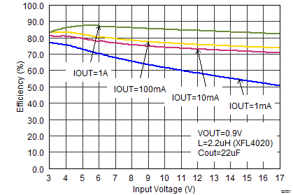
Figure 18.
Efficiency With 1.25 MHz, Vout = 0.9 V
Figure 20.
Output Voltage Accuracy (Load Regulation)
FSW=Low
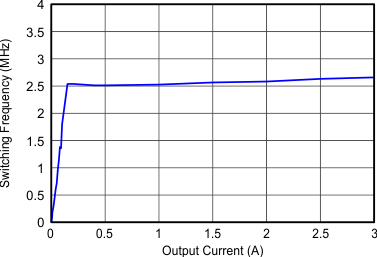
Figure 22.
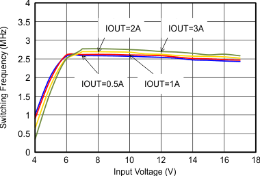
Switching Frequency
Figure 24.
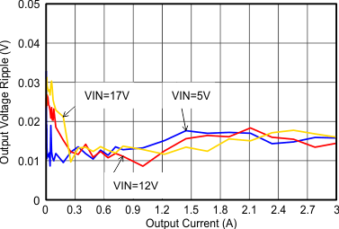
Output Voltage Ripple
Iout=1A
Figure 26.
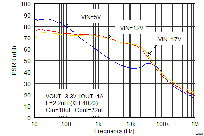
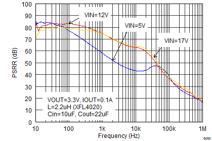
Power Supply Rejection Ratio, F
SW
= 2.5 MHz
Figure 28.
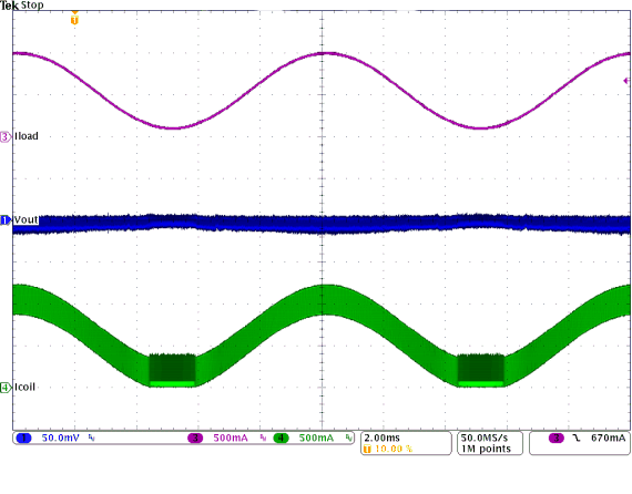
PWM-PSM-Transition
(V
IN
= 12 V, V
OUT
=3.3 V with 50 mV/Div)
Figure 30.
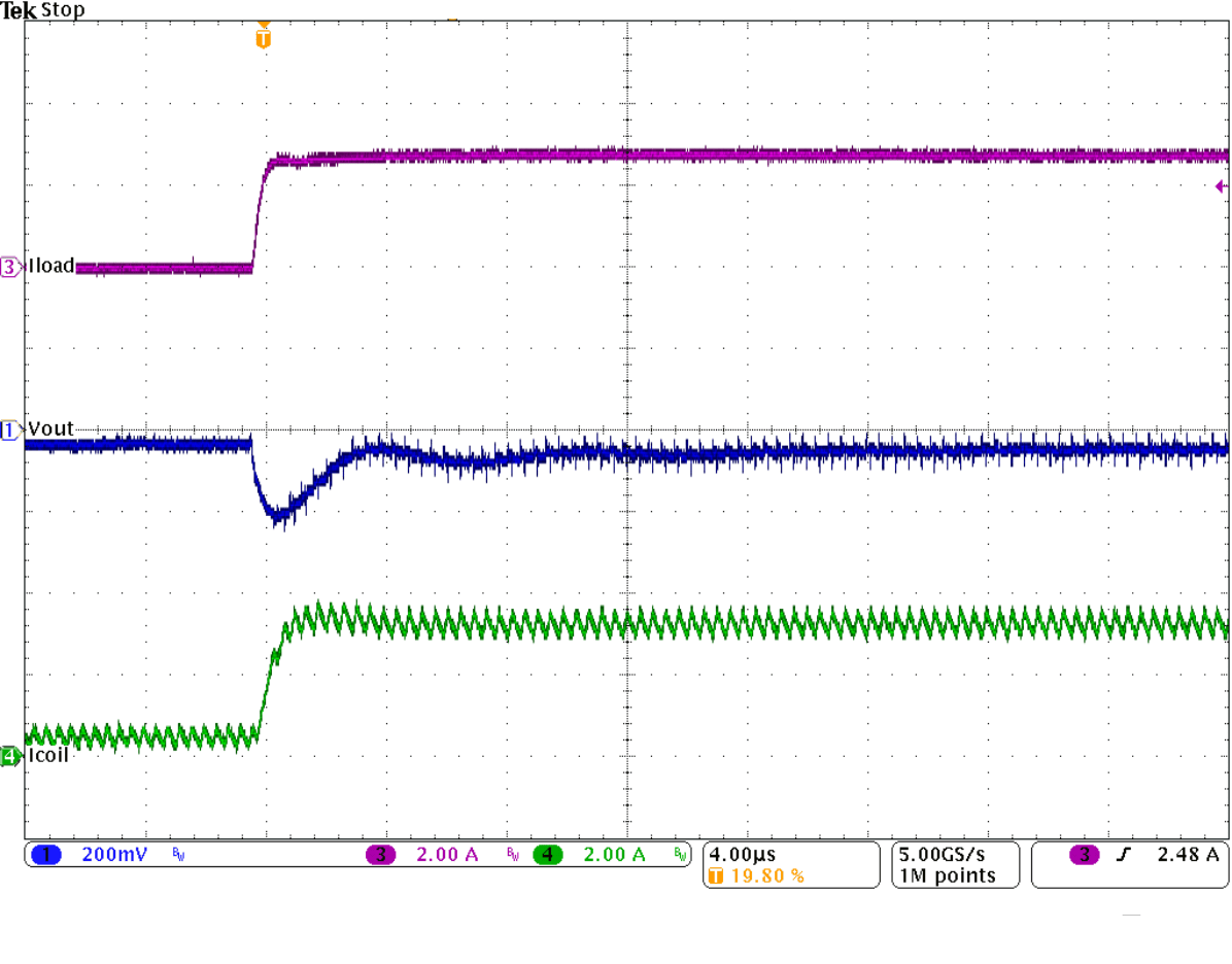
Load Transient Response of
Figure 29
,
Rising Edge
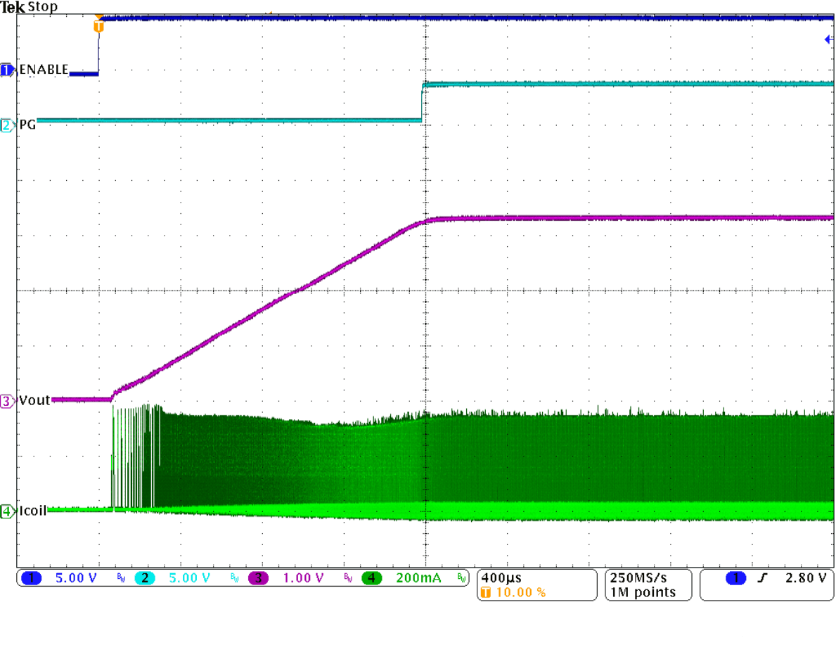
Figure 32.
Startup into 100 mA
Figure 34.
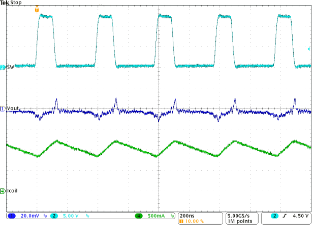
Typical Operation in PWM Mode
(I
OUT
= 1 A)
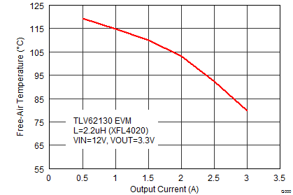
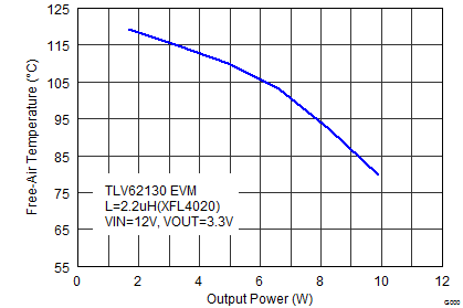
Figure 36.
Maximum Ambient Temperature (F
SW
= 2.5 MHz)
Figure 9.
Efficiency With 1.25 MHz, Vout = 5 V
Figure 11.
Efficiency With 2.5 MHz, Vout = 5 V
Figure 13.
Efficiency With 1.25 MHz, Vout = 3.3 V
Figure 15.
Efficiency With 2.5 MHz, Vout = 3.3 V
Figure 17.
Efficiency With 1.25 MHz, Vout = 1.8 V
Figure 19.
Efficiency With 1.25 MHz, Vout = 0.9 V
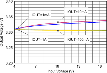
Figure 21.
Output Voltage Accuracy (Line Regulation)
FSW=Low
Figure 23.
Switching Frequency
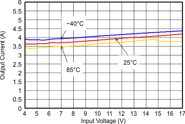
Figure 25.
Maximum Output Current
Iout=0.1A
Figure 27.
Power Supply Rejection Ratio, F
SW
= 2.5 MHz
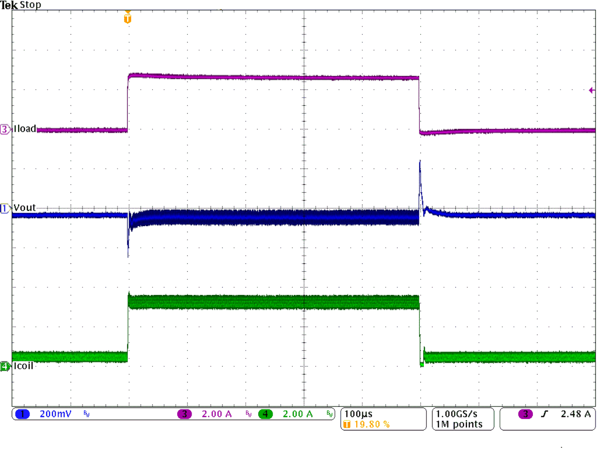
Figure 29.
Load Transient Response
(I
OUT
= 0.5 to 3 to 0.5 A)
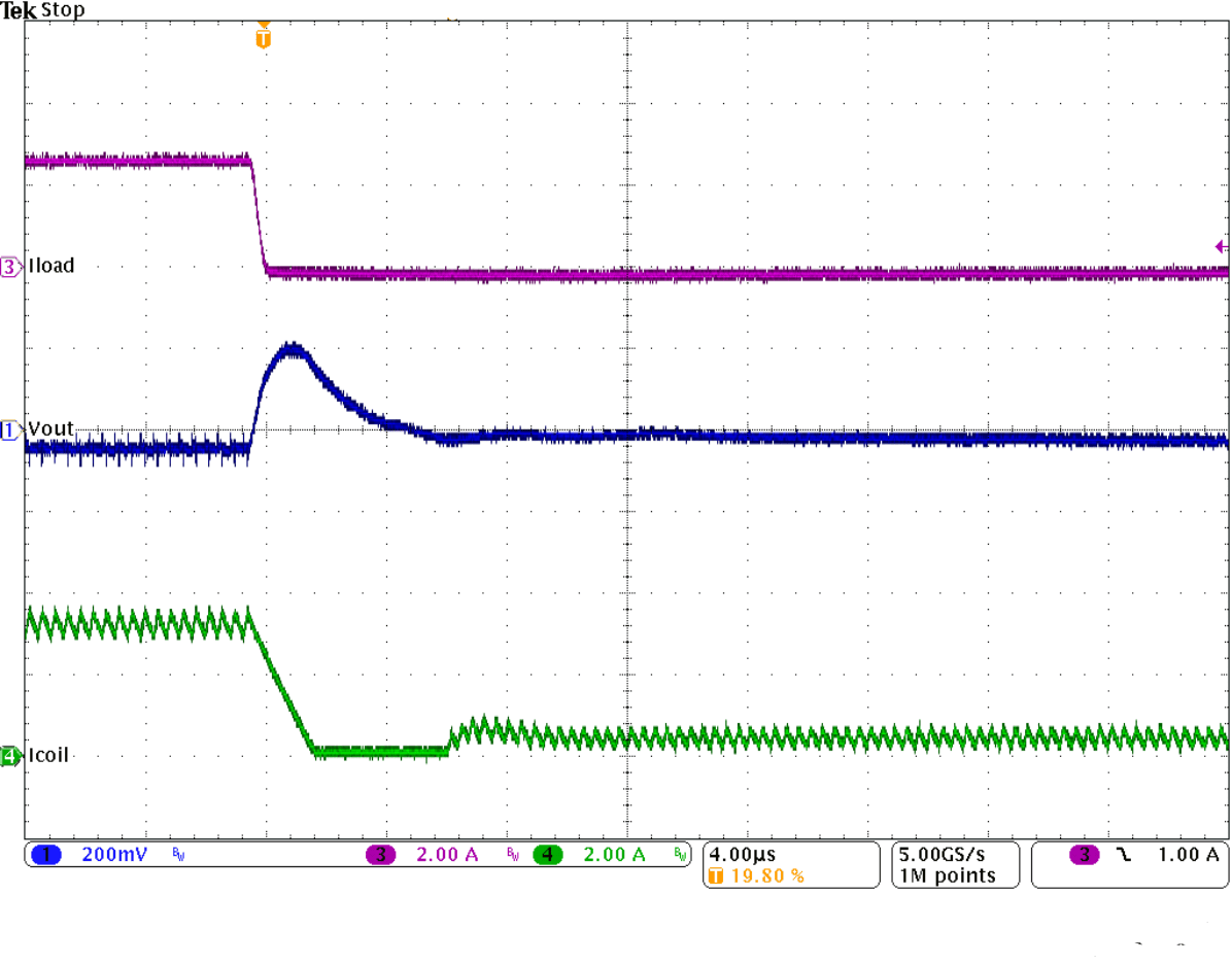
Figure 31.
Load Transient Response of
Figure 29
,
Falling Edge
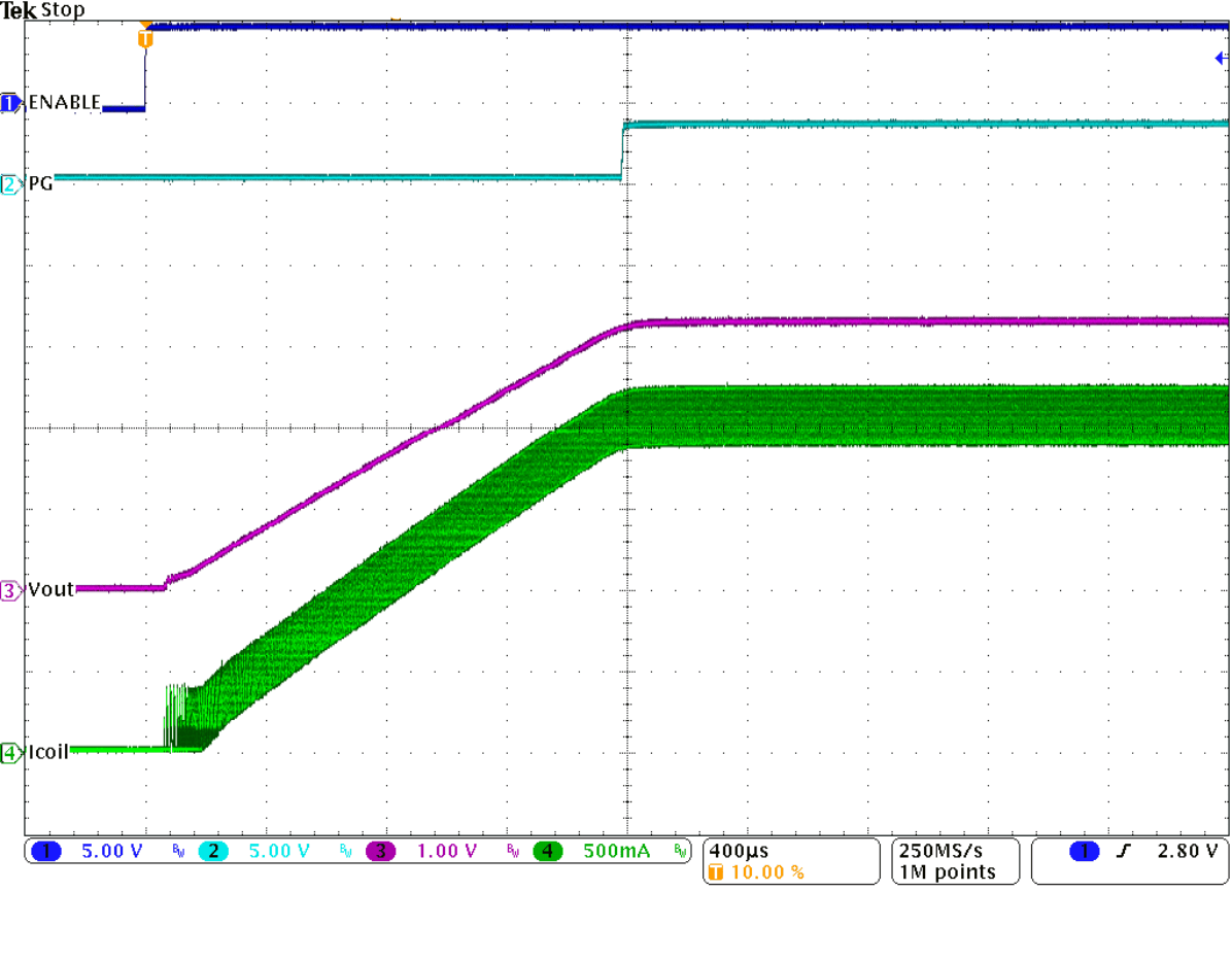
Figure 33.
Startup into 3 A
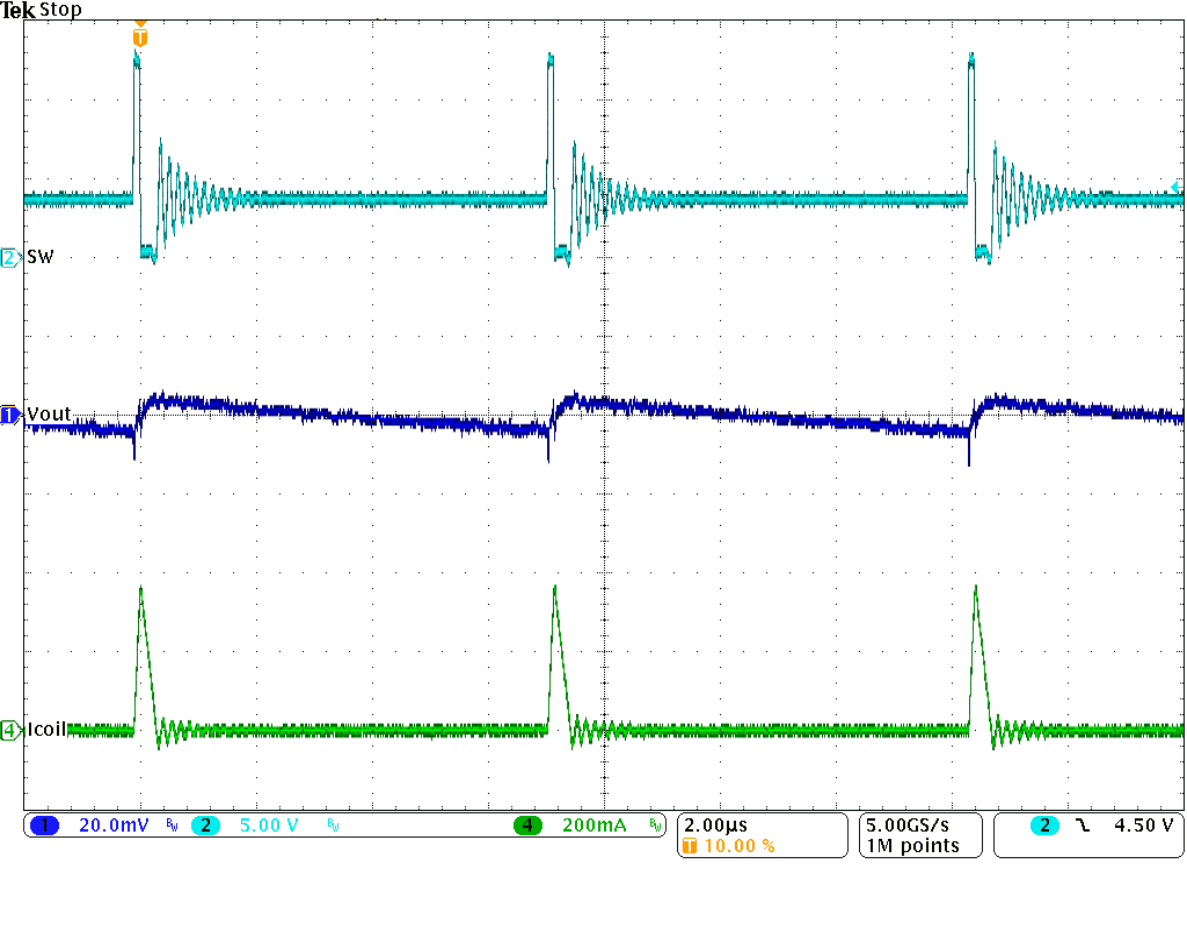
Figure 35.
Typical Operation in Power Save Mode
(I
OUT
= 10 mA)
Figure 37.
Maximum Ambient Temperature (F
SW
= 2.5 MHz)
sp