JAJSBR5H February   2012  – June 2018 TLV62130 , TLV62130A

PRODUCTION DATA.  

  1. 特長
  2. アプリケーション
  3. 概要
    1.     Device Images
      1.      代表的なアプリケーションの回路図
      2.      効率と出力電流との関係
  4. 改訂履歴
  5. Device Comparison Table
  6. Pin Configuration and Functions
    1.     Pin Functions
  7. Specifications
    1. 7.1 Absolute Maximum Ratings
    2. 7.2 ESD Ratings
    3. 7.3 Recommended Operating Conditions
    4. 7.4 Thermal Information
    5. 7.5 Electrical Characteristics
    6. 7.6 Typical Characteristics
  8. Detailed Description
    1. 8.1 Overview
    2. 8.2 Functional Block Diagram
    3. 8.3 Feature Description
      1. 8.3.1 Enable / Shutdown (EN)
      2. 8.3.2 Soft Start / Tracking (SS/TR)
      3. 8.3.3 Power Good (PG)
      4. 8.3.4 Pin-Selectable Output Voltage (DEF)
      5. 8.3.5 Frequency Selection (FSW)
      6. 8.3.6 Undervoltage Lockout (UVLO)
      7. 8.3.7 Thermal Shutdown
    4. 8.4 Device Functional Modes
      1. 8.4.1 Pulse Width Modulation (PWM) Operation
      2. 8.4.2 Power Save Mode Operation
      3. 8.4.3 100% Duty-Cycle Operation
      4. 8.4.4 Current Limit and Short Circuit Protection
  9. Application and Implementation
    1. 9.1 Application Information
    2. 9.2 Typical Application
      1. 9.2.1 Design Requirements
      2. 9.2.2 Detailed Design Procedure
        1. 9.2.2.1 Custom Design With WEBENCH® Tools
        2. 9.2.2.2 Programming the Output Voltage
        3. 9.2.2.3 External Component Selection
          1. 9.2.2.3.1 Inductor Selection
          2. 9.2.2.3.2 Capacitor Selection
            1. 9.2.2.3.2.1 Output Capacitor
            2. 9.2.2.3.2.2 Input Capacitor
            3. 9.2.2.3.2.3 Soft Start Capacitor
        4. 9.2.2.4 Tracking Function
        5. 9.2.2.5 Output Filter and Loop Stability
      3. 9.2.3 Application Curves
    3. 9.3 System Examples
      1. 9.3.1 LED Power Supply
      2. 9.3.2 Active Output Discharge
      3. 9.3.3 Inverting Power Supply
      4. 9.3.4 Various Output Voltages
  10. 10Power Supply Recommendations
  11. 11Layout
    1. 11.1 Layout Guidelines
    2. 11.2 Layout Example
    3. 11.3 Thermal Considerations
  12. 12デバイスおよびドキュメントのサポート
    1. 12.1 デバイス・サポート
      1. 12.1.1 デベロッパー・ネットワークの製品に関する免責事項
      2. 12.1.2 開発サポート
        1. 12.1.2.1 WEBENCH®ツールによるカスタム設計
    2. 12.2 ドキュメントの更新通知を受け取る方法
    3. 12.3 ドキュメントのサポート
      1. 12.3.1 関連資料
    4. 12.4 関連リンク
    5. 12.5 コミュニティ・リソース
    6. 12.6 商標
    7. 12.7 静電気放電に関する注意事項
    8. 12.8 Glossary
  13. 13メカニカル、パッケージ、および注文情報

Active Output Discharge

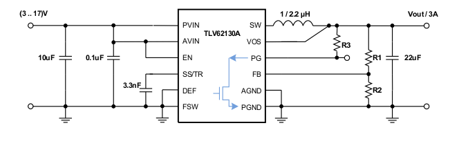
The TLV62130A pulls the PG pin Low, when the device is shut down by EN, UVLO or thermal shutdown. Connecting PG to Vout through a resistor can be used to discharge Vout in those cases (see Figure 39). The discharge rate can be adjusted by R3, which is also used to pull up the PG pin in normal operation. For reliability, keep the maximum current into the PG pin less than 10 mA.

spacing
TLV62130 TLV62130A SLVSB74_discharge.gifFigure 39. Discharge Vout Through PG Pin With TLV62130A