JAJSBW9A February   2013  – September 2024 UCC27532

PRODUCTION DATA  

  1.   1
  2. 特長
  3. アプリケーション
  4. 概要
  5. Pin Configuration and Functions
  6. Specifications
    1. 5.1 Absolute Maximum Ratings
    2. 5.2 Recommended Operating Conditions
    3. 5.3 Thermal Information
    4. 5.4 Electrical Characteristics
    5. 5.5 Typical Characteristics
  7. Detailed Description
    1. 6.1 Functional Block Diagram
    2. 6.2 Feature Description
      1. 6.2.1 VDD Under Voltage Lockout
      2. 6.2.2 Input Stage
      3. 6.2.3 Enable Function
      4. 6.2.4 Output Stage
      5. 6.2.5 Power Dissipation
    3. 6.3 Device Functional Modes
  8. Application and Implementation
    1. 7.1 Application Information
    2. 7.2 Typical Applications
  9. Layout
    1. 8.1 Layout Guidelines
    2. 8.2 Thermal Considerations
  10. Device and Documentation Support
    1. 9.1 サード・パーティ製品に関する免責事項
    2. 9.2 ドキュメントの更新通知を受け取る方法
    3. 9.3 サポート・リソース
    4. 9.4 Trademarks
    5. 9.5 静電気放電に関する注意事項
    6. 9.6 用語集
  11. 10Revision History
  12. 11Mechanical, Packaging, and Orderable Information

Functional Block Diagram

(EN Pull-Up Resistance to VREF = 500 kΩ, VREF = 5.8 V, In Pull-Down Resistance to GND = 230 kΩ)
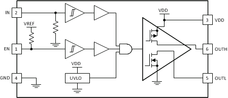
UCC27532