JAJSC15C December 2012 – March 2018 DRV2604
PRODUCTION DATA.
- 1 特長
- 2 アプリケーション
- 3 概要
- 4 改訂履歴
- 5 Pin Configuration and Functions
- 6 Specifications
-
7 Detailed Description
- 7.1 Overview
- 7.2 Functional Block Diagram
- 7.3
Feature Description
- 7.3.1 Support for ERM and LRA Actuators
- 7.3.2 Smart-Loop Architecture
- 7.3.3 Open-Loop Operation for LRA
- 7.3.4 Open-Loop Operation for ERM
- 7.3.5 Flexible Front-End Interface
- 7.3.6 Edge Rate Control
- 7.3.7 Constant Vibration Strength
- 7.3.8 Battery Voltage Reporting
- 7.3.9 One-Time Programmable (OTP) Memory for Configuration
- 7.3.10 Low-Power Standby
- 7.3.11 Device Protection
- 7.4 Device Functional Modes
- 7.5
Programming
- 7.5.1 Auto-Resonance Engine Programming for the LRA
- 7.5.2 Automatic-Level Calibration Programming
- 7.5.3 I2C Interface
- 7.5.4 Programming for Open-Loop Operation
- 7.5.5 Programming for Closed-Loop Operation
- 7.5.6 Auto Calibration Procedure
- 7.5.7 Programming On-Chip OTP Memory
- 7.5.8 Waveform Playback Programming
- 7.6
Register Map
- 7.6.1 Status (Address: 0x00)
- 7.6.2 Mode (Address: 0x01)
- 7.6.3 Real-Time Playback Input (Address: 0x02)
- 7.6.4 HI_Z (Address: 0x03)
- 7.6.5 Waveform Sequencer (Address: 0x04 to 0x0B)
- 7.6.6 GO (Address: 0x0C)
- 7.6.7 Overdrive Time Offset (Address: 0x0D)
- 7.6.8 Sustain Time Offset, Positive (Address: 0x0E)
- 7.6.9 Sustain Time Offset, Negative (Address: 0x0F)
- 7.6.10 Brake Time Offset (Address: 0x10)
- 7.6.11 Rated Voltage (Address: 0x16)
- 7.6.12 Overdrive Clamp Voltage (Address: 0x17)
- 7.6.13 Auto-Calibration Compensation Result (Address: 0x18)
- 7.6.14 Auto-Calibration Back-EMF Result (Address: 0x19)
- 7.6.15 Feedback Control (Address: 0x1A)
- 7.6.16 Control1 (Address: 0x1B)
- 7.6.17 Control2 (Address: 0x1C)
- 7.6.18 Control3 (Address: 0x1D)
- 7.6.19 Control4 (Address: 0x1E)
- 7.6.20 V(BAT) Voltage Monitor (Address: 0x21)
- 7.6.21 LRA Resonance Period (Address: 0x22)
- 7.6.22 RAM-Address Upper Byte (Address: 0xFD)
- 7.6.23 RAM-Address Lower Byte (Address: 0xFE)
- 7.6.24 RAM Data Byte (Address: 0xFF)
- 8 Application and Implementation
- 9 Power Supply Recommendations
- 10Layout
- 11デバイスおよびドキュメントのサポート
- 12メカニカル、パッケージ、および注文情報
10.1 Layout Guidelines
Use the following guidelines for the DRV2604 layout:
- The decoupling capacitor for the power supply (VDD) should be placed closed to the device pin.
- The filtering capacitor for the regulator (REG) should be placed close to the device REG pin.
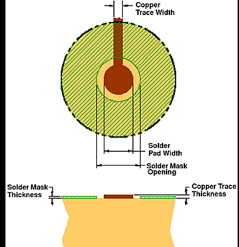
- When creating the pad size for the WCSP pins, TI recommends that the PCB layout use nonsolder mask-defined (NSMD) land. With this method, the solder mask opening is made larger than the desired land area and the opening size is defined by the copper pad width. Figure 61 shows and Table 29 lists appropriate diameters for a wafer-chip scale package (WCSP) layout.
 Figure 61. Land Pattern Dimensions
Table 29. Land Pattern Dimensions
| SOLDER PAD
DEFINITIONS |
COPPER PAD | SOLDER MASK
OPENING |
COPPER
THICKNESS |
STENCIL
OPENING |
STENCIL
THICKNESS |
|---|---|---|---|---|---|
| Nonsolder mask
defined (NSMD) |
275 µm
(0, –25 µm) |
375 µm
(0, –25 µm) |
1-oz maximum (32 µm) | 275 µm × 275 µm2
(rounded corners) |
125-µm thick |
- Circuit traces from NSMD defined PWB lands should be 75-µm to 100-µm wide in the exposed area inside the solder mask opening. Wider trace widths reduce device stand-off and impact reliability.
- The recommended solder paste is Type 3 or Type 4.
- The best reliability results are achieved when the PWB laminate glass transition temperature is above the operating the range of the intended application.
- For a PWB using a Ni/Au surface finish, the gold thickness should be less than 0.5 µm to avoid a reduction in thermal fatigue performance.
- Solder mask thickness should be less than 20 µm on top of the copper circuit pattern.
- The best solder stencil performance is achieved using laser-cut stencils with electro polishing. Use of chemically-etched stencils results in inferior solder paste volume control.
- Trace routing away from the WCSP device should be balanced in X and Y directions to avoid unintentional component movement because of solder-wetting forces.