JAJSC20A October 2015 – May 2016 LM5175
PRODUCTION DATA.
- 1 特長
- 2 アプリケーション
- 3 概要
- 4 概略回路図
- 5 改訂履歴
- 6 Pin Configuration and Functions
- 7 Specifications
-
8 Detailed Description
- 8.1 Overview
- 8.2 Functional Block Diagram
- 8.3
Feature Description
- 8.3.1 Fixed Frequency Valley/Peak Current Mode Control with Slope Compensation
- 8.3.2 VCC Regulator and Optional BIAS Input
- 8.3.3 Enable/UVLO
- 8.3.4 Soft-Start
- 8.3.5 Overcurrent Protection
- 8.3.6 Average Input/Output Current Limiting
- 8.3.7 CCM/DCM Operation
- 8.3.8 Frequency and Synchronization (RT/SYNC)
- 8.3.9 Frequency Dithering
- 8.3.10 Output Overvoltage Protection (OVP)
- 8.3.11 Power Good (PGOOD)
- 8.3.12 Gm Error Amplifier
- 8.3.13 Integrated Gate Drivers
- 8.3.14 Thermal Shutdown
- 8.4 Device Functional Modes
-
9 Application and Implementation
- 9.1 Application Information
- 9.2
Typical Application
- 9.2.1 Design Requirements
- 9.2.2
Detailed Design Procedure
- 9.2.2.1 Frequency
- 9.2.2.2 VOUT
- 9.2.2.3 Inductor Selection
- 9.2.2.4 Output Capacitor
- 9.2.2.5 Input Capacitor
- 9.2.2.6 Sense Resistor (RSENSE)
- 9.2.2.7 Slope Compensation
- 9.2.2.8 UVLO
- 9.2.2.9 Soft-Start Capacitor
- 9.2.2.10 Dither Capacitor
- 9.2.2.11 MOSFETs QH1 and QL1
- 9.2.2.12 MOSFETs QH2 and QL2
- 9.2.2.13 Frequency Compensation
- 9.2.3 Application Curves
- 10Power Supply Recommendations
- 11Layout
- 12デバイスおよびドキュメントのサポート
- 13メカニカル、パッケージ、および注文情報
8 Detailed Description
8.1 Overview
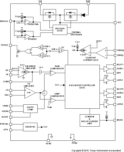
The LM5175 is a wide input voltage four-switch buck-boost controller IC with integrated drivers for N-channel MOSFETs. It operates in the buck mode when VIN is greater than VOUT and in the boost mode when VIN is less than VOUT. When VIN is close to VOUT, the device operates in a proprietary transition buck or boost mode. The control scheme provides smooth operation for any input/output combination within the specified operating range. The buck or boost transition control scheme provides a low ripple output voltage when VIN equals VOUT without compromising the efficiency.
The LM5175 integrates four N-Channel MOSFET drivers including two low-side drivers and two high-side drivers, eliminating the need for external drivers or floating bias supplies. The internal VCC regulator supplies internal bias rails as well as the MOSFET gate drivers. The VCC regulator is powered either from the input voltage through the VIN pin or from the output or an external supply through the BIAS pin for improved efficiency.
The PWM control scheme is based on valley current mode control for buck operation and peak current mode control for boost operation. The inductor current is sensed through a single sense resistor in series with the low-side MOSFETs. The sensed current is also monitored for cycle-by-cycle current limit. The behavior of the LM5175 during an overload condition is dependent on the MODE pin programming (see MODE Pin Configuration). If hiccup mode fault protection is selected, the controller turns off after a fixed number of switching cycles in cycle-by-cycle current limit and restarts after another fixed number of clock cycles. The hiccup mode reduces the heating in the power components in a sustained overload condition. If hiccup mode is disabled through the MODE pin, the controller remains in a cycle-by-cycle current limit condition until the overload is removed. The MODE pin also selects continuous conduction mode (CCM) for noise sensitive applications or discontinuous conduction mode (DCM) for higher light load efficiency.
In addition to the cycle-by-cycle current limiting, the LM5175 also provides an optional average current regulation loop that can be configured for either input or output current limiting. This is useful for battery charging or other applications where a constant current behavior may be required.
The soft-start time of LM5175 is programmed by a capacitor connected to the SS pin to minimize the inrush current and overshoot during startup.
The precision EN/UVLO pin supports programmable input undervoltage lockout (UVLO) with hysteresis. The output overvoltage protection (OVP) feature turns off the high-side drivers when the voltage at the FB pin is 7.5% above the nominal 0.8-V VREF. The PGOOD output indicates when the FB voltage is inside a ±10% regulation window centered at VREF.
8.2 Functional Block Diagram
8.3 Feature Description
8.3.1 Fixed Frequency Valley/Peak Current Mode Control with Slope Compensation
The LM5175 implements a fixed frequency current mode control of both the buck and boost switches. The output voltage, scaled down by the feedback resistor divider, appears at the FB pin and is compared to the internal reference (VREF) by an internal error amplifier. The error amplifier produces an error voltage by driving the COMP pin. An adaptive slope compensation signal based on VIN, VOUT, and the capacitor at the SLOPE pin is added to the current sense signal measured across the CS and CSG pins. The result is compared to the COMP error voltage by the PWM comparator.
The LM5175 regulates the output using valley current mode control in buck mode and peak current mode control in boost mode. For valley current mode control, the high-side buck MOSFET controlled by HDRV1 is turned on by the PWM comparator at the valley of the inductor ripple current and turned off by the oscillator clock signal. Valley current mode control is advantageous for buck converters where the PWM controller must resolve very short on-times. For peak current mode control in the boost mode, the low-side boost MOSFET controlled by LDRV2 is turned on by the clock signal in each switching cycle and turned off by the PWM comparator at the peak of the inductor ripple current.
The low-side gate drive LDRV1, complementary to the HDRV1 drive signal, controls the synchronous rectification MOSFET of the buck stage. The high-side gate drive HDRV2, complementary to the low-side gate drive LDRV2, controls the high-side synchronous rectifier of the boost stage. For operation with VIN close to VOUT, the LM5175 uses a proprietary buck or boost transition scheme to achieve smooth, low ripple transition zone behavior.
Peak and valley current mode controllers require slope compensation for stable current loop operation at duty cycle greater than 50% in peak current mode control and less than 50% in valley current mode control. The LM5175 provides a SLOPE pin to program optimum slope for any VIN and VOUT combination using an external capacitor.
8.3.2 VCC Regulator and Optional BIAS Input
The VCC regulator provides a regulated 7.5-V bias supply to the gate drivers. When EN/UVLO is above the 0.7-V (typical) standby threshold, the VCC regulator is turned on. For VIN less than 7.5 V, the VCC voltage tracks VIN with a small voltage drop as shown in Figure 4. If the EN/UVLO input is above the 1.23 V operating threshold and VCC exceeds the 3.3 V (typical) VCC UV threshold, the controller is enabled and switching begins.
The VCC regulator draws power from VIN when there is no supply voltage connected to the BIAS pin. If the BIAS pin is connected to an external voltage source that exceeds VCC by one diode drop, the VCC regulator draws power from the BIAS input instead of VIN. Connecting the BIAS pin to VOUT in applications with VOUT greater than 8.5 V improves the efficiency of the regulator in the buck mode. The BIAS pin voltage should not exceed 36 V.
For low VIN operation, ensure that the VCC voltage is sufficient to fully enhance the MOSFETs. Use an external bias supply if VIN dips below the voltage required to sustain the VCC voltage. For these conditions, use a series blocking diode between the input supply and the VIN pin (Figure 20). This prevents VCC from back-feeding into VIN through the body diode of the VCC regulator.
A 1-µF capacitor to PGND is required to supply the VCC regulator load transients.
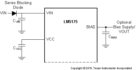 Figure 20. VCC Regulator
8.3.3 Enable/UVLO
The LM5175 has a dual function enable and undervoltage lockout (UVLO) circuit. The EN/UVLO pin has three distinct voltage ranges: shutdown, standby, and operating (see Shutdown, Standby, and Operating Modes). When the EN/UVLO pin is below the standby threshold (0.7 V typical), the converter is held in a low power shutdown mode. When EN/UVLO voltage is greater than the standby threshold but less than the 1.23 V operating threshold, the internal bias rails and the VCC regulator are enabled but the soft-start (SS) pin is held low and the PWM controller is disabled. A 1.5 µA pull-up current is sourced out of the EN/UVLO pin in standby mode to provide hysteresis between the shutdown mode and the standby mode. When EN/UVLO is greater than the 1.23 V operating threshold, the controller commences operation if VCC is above VCC UV threshold (3.3 V). A hysteresis current of 3.5 µA is sourced into the EN/UVLO pin when the EN/UVLO input exceeds the 1.23 V operation threshold to provide hysteresis that prevents on/off chattering in the presence of noise with a slowly changing input voltage.
The VIN undervoltage lockout turn-on threshold is typically set by a resistor divider from the VIN pin to AGND with the mid-point of the divider connected to EN/UVLO. The turn-on threshold VINUV is calculated using Equation 1 where RUV2 is the upper resistor and RUV1 is the lower resistor in the EN/UVLO resistor divider:

The hysteresis between the UVLO turn-on threshold and turn-off threshold is set by the upper resistor in the EN/UVLO resistor divider and is given by:

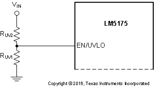 Figure 21. UVLO Threshold Programming
8.3.4 Soft-Start
The LM5175 soft-start time is programmed using a soft-start capacitor from the SS pin to AGND. When the converter is enabled, an internal 5-µA current source charges the soft-start capacitor. When the SS pin voltage is below the 0.8-V feedback reference voltage VREF, the soft-start pin controls the regulated FB voltage. Once SS exceeds VREF, the soft-start interval is complete and the error amplifier is referenced to VREF. The soft-start time is given by Equation 3:

The soft-start capacitor is internally discharged when the converter is disabled because of EN/UVLO falling below the operation threshold or VCC falling below the VCC UV threshold. The soft-start pin is also discharged when the converter is in hiccup mode current limiting or in thermal shutdown. When average input or output current limiting is active, the soft-start capacitor is discharged by the constant current loop transconductance (gm) amplifier to limit either input or output current.
8.3.5 Overcurrent Protection
The LM5175 provides cycle-by-cycle current limit to protect against overcurrent and short circuit conditions. In buck operation, the sensed valley voltage across the CSG and CS pins is limited to 76 mV. The high-side buck switch skips a cycle if the sensed voltage does not fall below this threshold during the buck switch off time. In boost operation, the maximum peak voltage across CS and CSG is limited to 170mV. If the peak current in the low-side boost switch causes the CS pin to exceed this threshold voltage, the boost switch is turned off for the remainder of the clock cycle.
Applying the appropriate voltage to the MODE pin of the LM5175 enables hiccup mode fault protection (see MODE Pin Configuration). In the hiccup mode, the controller shuts down after detecting cycle-by-cycle current limiting for 128 consecutive cycles and the soft-start capacitor is discharged. The soft-start capacitor is automatically released after 4000 oscillator clock cycles and the controller restarts. If hiccup mode protection is not enabled through the MODE pin, the LM5175 will operate in cycle-by-cycle current limiting as long as the overload condition persists.
8.3.6 Average Input/Output Current Limiting
The LM5175 provides optional average current limiting capability to limit either the input or the output current of the DC/DC converter. The average current limiting circuit uses an additional current sense resistor connected in series with the input supply or output voltage of the converter. A current sense gm amplifier with inputs at the ISNS(+) and ISNS(-) pins monitors the voltage across the sense resistor and compares it with an internal 50 mV reference. If the drop across the sense resistor is greater than 50 mV, the gm amplifier gradually discharges the soft-start capacitor. When the soft-start capacitor discharges below the 0.8-V feedback reference voltage VREF, the output voltage of the converter decreases to limit the input or output current. The average current limiting feature can be used in applications requiring a regulated current from the input supply or into the load. The target constant current is given by Equation 4:

The average current loop can be disabled by shorting the ISNS(+) and ISNS(-) pins together.
8.3.7 CCM/DCM Operation
The LM5175 allows selection of continuous conduction mode (CCM) or discontinuous conduction mode (DCM) operation using the MODE pin (see MODE Pin Configuration). In CCM operation the inductor current can flow in either direction and the controller switches at a fixed frequency regardless of the load current. This mode is useful for noise-sensitive applications where a fixed switching eases filter design. In DCM operation the synchronous rectifier MOSFETs emulate diodes as LDRV1 or HDRV2 turn-off for the remainder of the PWM cycle when the inductor current reaches zero. The DCM mode results in reduced frequency operation at light loads, which lowers switching losses and increases light load efficiency of the converter.
8.3.8 Frequency and Synchronization (RT/SYNC)
The LM5175 switching frequency can be programmed between 100 kHz and 600 kHz using a resistor from the RT/SYNC pin to AGND. The RT resistor is related to the nominal switching frequency (Fsw) by the following equation:

Figure 3 in the Typical Characteristics shows the relationship between the programmed switching frequency (Fsw) and the RT resistor.
The RT/SYNC pin can also be used for synchronizing the internal oscillator to an external clock signal. The external synchronization pulse is ac coupled using a capacitor to the RT/SYNC pin. The voltage at the RT/SYNC pin must not exceed 3.3 V peak. The external synchronization pulse frequency should be higher than the internally set oscillator frequency and the pulse width should be between 75 ns and 500 ns.
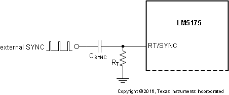 Figure 22. Using External SYNC
8.3.9 Frequency Dithering
The LM5175 provides an optional frequency dithering function that is enabled by connecting a capacitor from DITH to AGND. Figure 23 illustrates the dithering circuit. A triangular waveform centered at 1.22 V is generated across the CDITH capacitor. This triangular waveform modulates the oscillator frequency by ±5% of the nominal frequency set by the RT resistor. The CDITH capacitance value sets the rate of the low frequency modulation. A lower CDITH capacitance will modulate the oscillator frequency at a faster rate than a higher capacitance. For the dithering circuit to effectively reduce peak EMI, the modulation rate must be much less than the oscillator frequency (Fsw). Equation 6 calculates the DITH pin capacitance required to set the modulation frequency, FMOD. Connecting the DITH pin directly to AGND disables frequency dithering, and the internal oscillator operates at a fixed frequency set by the RT resistor. Dither is disabled when external SYNC is used.

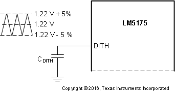 Figure 23. Dither Operation
8.3.10 Output Overvoltage Protection (OVP)
The LM5175 provides an output overvoltage protection (OVP) circuit that turns off the gate drives when the feedback voltage is 7.5% above the 0.8 V feedback reference voltage VREF. Switching resumes once the output falls within 5% of VREF.
8.3.11 Power Good (PGOOD)
PGOOD is an open drain output that is pulled low when the voltage at the FB pin is outside -9% / +10% of the nominal 0.8-V reference voltage. The PGOOD internal N-Channel MOSFET pull-down strength is typically 4.2 mA. This pin can be connected to a voltage supply of up to 8 V through a pull-up resistor.
8.3.12 Gm Error Amplifier
The LM5175 has a gm error amplifier for loop compensation. The gm amplifier output (COMP) range is 0.3 V to 3 V. Connect an Rc1-Cc1 compensation network between COMP and ground for type II (PI) compensation (see Figure 24). Another pole is usually added using Cc2 to suppress higher frequency noise.
The COMP output voltage (VCOMP) range limits the possible VIN and IOUT range for a given design. In buck mode, the maximum VIN for which the converter can regulate the output at no load is when VCOMP reaches 0.3 V. Equation 7 gives VCOMP as a function of VIN at no load in CCM buck mode:
Where DBUCK in the equation Equation 7 is the buck duty cycle given by:

A larger L1, lower slope ripple (higher CSLOPE), smaller sense resistor (RSENSE), and higher frequency can increase the maximum VIN range for buck operation.
For boost mode, the minimum VIN for which the converter can regulate the output at full load is when VCOMP reaches 3 V. Equation 9 gives VCOMP as a function of VIN in boost mode:

Where DBOOST in the Equation 9 is the boost duty cycle given by:

A larger L1, lower slope ripple (higher CSLOPE), smaller sense resistor (RSENSE), and higher frequency can extend the minimum VIN range for boost operation.
8.3.13 Integrated Gate Drivers
The LM5175 provides four N-channel MOSFET gate drivers: two floating high-side gate drivers at the HDRV1 and HDRV2 pins, and two ground referenced low-side drivers at the LDRV1 and LDRV2 pins. Each driver is capable of sourcing 1.5 A and sinking 2 A peak current. In buck operation, LDRV1 and HDRV1 are switched by the PWM controller while HDRV2 remains continuously on. In boost operation, LDRV2 and HDRV2 are switched while HDRV1 remains continuously on.
In DCM buck operation, LDRV1 and HDRV2 turn off when the inductor current drops to zero (diode emulation). In a DCM boost operation, HDRV2 turns off when inductor current drops to zero.
The gate drive output HDRV2 remains off during soft-start to prevent reverse current flow from a pre-biased output.
The low-side gate drivers are powered from VCC and the high-side gate drivers HDRV1 and HDRV2 are powered from bootstrap capacitors CBOOT1 (between BOOT1 and SW1) and CBOOT2 (between BOOT2 and SW2) respectively. The CBOOT1 and CBOOT2 capacitors are charged through external Schottky diodes connected to the VCC pin as shown in Figure 24.
8.3.14 Thermal Shutdown
The LM5175 is protected by a thermal shutdown circuit that shuts down the device when the internal junction temperature exceeds 165°C (typical). The soft-start capacitor is discharged when thermal shutdown is triggered and the gate drivers are disabled. The converter automatically restarts when the junction temperature drops by the thermal shutdown hysteresis of 15°C below the thermal shutdown threshold.
8.4 Device Functional Modes
Please refer to Enable/UVLO section for the description of EN/UVLO pin function. Shutdown, Standby, and Operating Modes section lists the shutdown, standby, and operating modes for LM5175 as a function of EN/UVLO and VCC voltages.
8.4.1 Shutdown, Standby, and Operating Modes
8.4.2 MODE Pin Configuration
The MODE pin is used to select CCM/DCM operation and hiccup mode current limit. Mode is latched at startup.
| MODE PIN CONNECTION | LIGHT LOAD MODE | HICCUP FAULT PROTECTION |
|---|---|---|
| Connect to VCC | CCM | No Hiccup |
| RMODE to AGND = 93.1 kΩ | CCM | Hiccup Enabled |
| RMODE to AGND = 49.9 kΩ | DCM | Hiccup Enabled |
| Connect to AGND | DCM | No Hiccup |
