JAJSC56F
December 2012 – March 2018
UCC27611
PRODUCTION DATA.
1
特長
2
アプリケーション
3
概要
Device Images
代表的なアプリケーションの図
4
改訂履歴
5
Pin Configuration and Functions
Pin Functions
6
Specifications
6.1
Absolute Maximum Ratings
6.2
ESD Ratings
6.3
Recommended Operating Conditions
6.4
Thermal Information
6.5
Electrical Characteristics
6.6
Switching Characteristics
6.7
Typical Characteristics
7
Detailed Description
7.1
Overview
7.2
Functional Block Diagram
7.3
Feature Description
7.3.1
VDD and Undervoltage Lockout
7.3.2
Operating Supply Current
7.3.3
Input Stage
7.3.4
Enable Function
7.3.5
Output Stage
7.3.6
Low Propagation Delays
7.4
Device Functional Modes
8
Application and Implementation
8.1
Application Information
8.2
Typical Application
8.2.1
Design Requirements
8.2.2
Detailed Design Procedure
8.2.2.1
Gate Drive Supply Voltage
8.2.2.2
Input Configuration
8.2.2.3
Output Configuration
8.2.2.4
Power Dissipation
8.2.2.5
Thermal Considerations
8.2.3
Application Curves
9
Power Supply Recommendations
10
Layout
10.1
Layout Guidelines
10.2
Layout Example
11
デバイスおよびドキュメントのサポート
11.1
ドキュメントのサポート
11.1.1
関連資料
11.2
ドキュメントの更新通知を受け取る方法
11.3
コミュニティ・リソース
11.4
商標
11.5
静電気放電に関する注意事項
11.6
Glossary
12
メカニカル、パッケージ、および注文情報
8.2.3
Application Curves
Figure 14.
Output Rising
(Ch1 = IN+, Ch2 = OUTPUT)
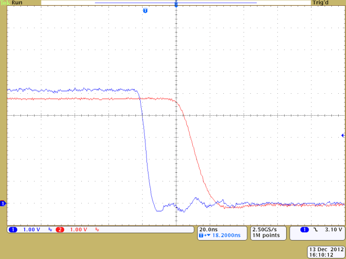
Figure 15.
Output Falling
(Ch1 = IN+, Ch2 = OUTPUT)