JAJSCD1B June   2016  – March 2019 TPS63070

PRODUCTION DATA.  

  1. 特長
  2. アプリケーション
  3. 概要
    1.     Device Images
      1.      概略回路図
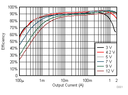
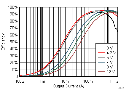
      2.      効率と出力電流との関係、、Vo = 5V
  4. 改訂履歴
  5. Device Comparison Table
  6. Pin Configuration and Functions
    1.     Pin Functions
  7. Specifications
    1. 7.1 Absolute Maximum Ratings
    2. 7.2 ESD Ratings
    3. 7.3 Recommended Operating Conditions
    4. 7.4 Thermal Information
    5. 7.5 Electrical Characteristics
    6. 7.6 Typical Characteristics
  8. Detailed Description
    1. 8.1 Overview
    2. 8.2 Functional Block Diagram TPS63070
    3. 8.3 Functional Block Diagram TPS630701
    4. 8.4 Feature Description
      1. 8.4.1  Control Loop Description
      2. 8.4.2  Precise Enable
      3. 8.4.3  Power Good
      4. 8.4.4  Soft Start
      5. 8.4.5  PS/SYNC
      6. 8.4.6  Short Circuit Protection
      7. 8.4.7  VSEL and FB2 pins
      8. 8.4.8  Overvoltage Protection
      9. 8.4.9  Undervoltage Lockout
      10. 8.4.10 Overtemperature Protection
    5. 8.5 Device Functional Modes
      1. 8.5.1 Power Save Mode
      2. 8.5.2 Current Limit
      3. 8.5.3 Output Discharge Function (TPS630702 only)
  9. Application and Implementation
    1. 9.1 Application Information
    2. 9.2 Typical Application for adjustable version
      1. 9.2.1 Design Requirements
      2. 9.2.2 Detailed Design Procedure
        1. 9.2.2.1 Programming The Output Voltage
        2. 9.2.2.2 Inductor Selection
        3. 9.2.2.3 Capacitor Selection
          1. 9.2.2.3.1 Input Capacitor
          2. 9.2.2.3.2 Output Capacitor
      3. 9.2.3 Application Curves
    3. 9.3 Typical Application for Fixed Voltage Version
      1. 9.3.1 Design Requirements
      2. 9.3.2 Detailed Design Procedure
      3. 9.3.3 Application Curves
  10. 10Power Supply Recommendations
    1. 10.1 Thermal Information
  11. 11Layout
    1. 11.1 Layout Guidelines
    2. 11.2 Layout Example
  12. 12デバイスおよびドキュメントのサポート
    1. 12.1 デバイス・サポート
      1. 12.1.1 デベロッパー・ネットワークの製品に関する免責事項
    2. 12.2 関連リンク
    3. 12.3 ドキュメントの更新通知を受け取る方法
    4. 12.4 コミュニティ・リソース
    5. 12.5 商標
    6. 12.6 静電気放電に関する注意事項
    7. 12.7 Glossary
  13. 13メカニカル、パッケージ、および注文情報

Application Curves

Table 9. Typical Application Curves for Fixed Voltage Version

Parameter Conditions Figure
Efficiency
Efficiency vs Output Current (PFM/PWM) VIN = 3 V, 4.2 V, 5 V, 7 V, 9 V, 12 V, VOUT = 5 V , PS/SYNC = Low Figure 38
Efficiency vs Output Current (PWM only) VIN = 3 V, 4.2 V, 5 V, 7 V, 9 V, 12 V, VOUT = 5 V , PS/SYNC = High Figure 39
Load Regulation
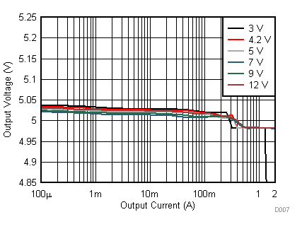
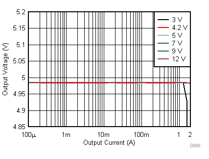
Load Regulation, PFM/PWM Operation VIN = 3 V, 4.2 V, 5 V, 7 V, 9 V, 12 V, VOUT = 5 V , PS/SYNC = Low Figure 40
Load Regulation, PWM Operation VIN = 3 V, 4.2 V, 5 V, 7 V, 9 V, 12 V, VOUT = 5 V , PS/SYNC = High Figure 41
Output Current
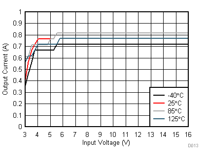
Typical Start-up Current vs Input Voltage VOUT = 5 V, TJ = -40 °C, 25 °C, 85 °C, 125 °C Figure 42
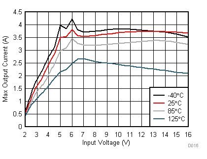
Maximum Load Current vs Input Voltage VOUT = 5 V, TJ = -40 °C, 25 °C, 85 °C, 125 °C, PG = high Figure 43
Regulation Accuracy
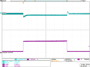
Load Transient, PFM/PWM Boost Operation VIN = 4.2 V, VOUT = 5 V, Load = 100 mA to 1 A, PS/SYNC = Low Figure 44
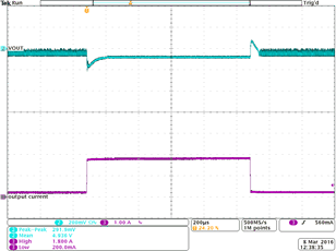
Load Transient, PFM/PWM Buck Operation VIN = 12 V, VOUT = 5 V, Load = 200 mA to 1.8 A, PS/SYNC = Low Figure 45
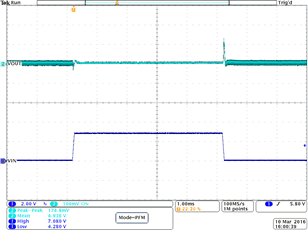
Line Transient, PFM/PWM Operation VIN = 4.2 V to 7 V, VOUT = 5 V, Load = 1 A, PS/SYNC = Low Figure 46
Output Voltage Ripple
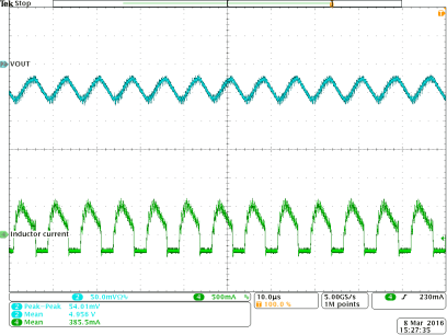
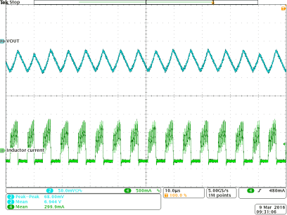
Output Voltage Ripple, PFM/PWM Operation VIN = 4.2 V, VOUT = 5 V, Load = 0.3 A, PS/SYNC = Low Figure 47
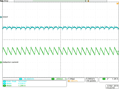
Output Voltage Ripple, PWM Operation VIN = 4.2 V, VOUT = 5 V, Load = 1 A, PS/SYNC = high Figure 48
Output Voltage Ripple, PFM/PWM Operation VIN = 7.2 V, VOUT = 5 V, Load = 0.3 A, PS/SYNC = Low Figure 49
Startup
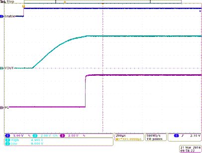
Start-up Behavior from Rising Enable, PFM/PWM Operation VIN = 4.5 V, VOUT = 5 V, Load = 0.5 A, PS/SYNC = Low Figure 50
TPS63070 D001_SLVSC58.gif
Vout = 5 V PFM T = 25 °C
Figure 38. Efficiency vs Output Current
TPS63070 D007_SLVSC58.gif
Vout = 5 V PFM T = 25 °C
Figure 40. Output Voltage vs Output Current
TPS63070 D013_SLVSC58.gif
Vout = 5 V resistive load
Figure 42. Typical Start-up Current
TPS63070 Load_Trans_5V_PFM_VIN4V2.gif
Vout = 5 V PFM Vin = 4.2V
Figure 44. Load Transient Response
TPS63070 Line_Trans_5V.gif
Vout = 5 V PFM Io = 1A
Figure 46. Line Transient Response
TPS63070 35_TPS63070_VOUT_Ripple_5V0_PWM_4p2V_1A.gif
Vin = 4.2V; Vout = 5 V PWM Io = 1A
Figure 48. Output Voltage Ripple
TPS63070 22_TPS63070_startup_timingVIN4V5_Vo5V.gif
Vin = 4.5V; Vout = 5 V PFM Io = 0.5A
Figure 50. Start-up Timing
TPS63070 D002_SLVSC58.gif
Vout = 5 V PWM T = 25 °C
Figure 39. Efficiency vs Output Current
TPS63070 D008_SLVSC58.gif
Vout = 5 V PWM T = 25 °C
Figure 41. Output Voltage vs Output Current
TPS63070 D016_SLVSC58.gif
Vout = 5 V after start-up with PG = high
Figure 43. Maximum Load Current vs Input Voltage
TPS63070 Load_Trans_5V_PFM_VIN12V.gif
Vout = 5 V PFM Vin = 12V
Figure 45. Load Transient Response
TPS63070 34_TPS63070_VOUT_Ripple_5V0_PFM_4p2V_0p3A.gif
Vin = 4.2V; Vout = 5 V PFM Io = 0.3A
Figure 47. Output Voltage Ripple
TPS63070 39_TPS63070_VOUT_Ripple_7V0_PFM_12V_0p3A.gif
Vin = 7.2V; Vout = 5 V PFM Io = 0.3A
Figure 49. Output Voltage Ripple