JAJSCH2A September 2016 – June 2017 ADS9120
PRODUCTION DATA.
- 1 特長
- 2 アプリケーション
- 3 概要
- 4 改訂履歴
- 5 Pin Configuration and Functions
-
6 Specifications
- 6.1 Absolute Maximum Ratings
- 6.2 ESD Ratings
- 6.3 Recommended Operating Conditions
- 6.4 Thermal Information
- 6.5 Electrical Characteristics
- 6.6 Timing Requirements: Conversion Cycle
- 6.7 Timing Requirements: Asynchronous Reset, NAP, and PD
- 6.8 Timing Requirements: SPI-Compatible Serial Interface
- 6.9 Timing Requirements: Source-Synchronous Serial Interface (External Clock)
- 6.10 Timing Requirements: Source-Synchronous Serial Interface (Internal Clock)
- 6.11 Typical Characteristics
-
7 Detailed Description
- 7.1 Overview
- 7.2 Functional Block Diagram
- 7.3 Feature Description
- 7.4 Device Functional Modes
- 7.5
Programming
- 7.5.1 Data Transfer Frame
- 7.5.2 Interleaving Conversion Cycles and Data Transfer Frames
- 7.5.3 Data Transfer Protocols
- 7.5.4 Device Setup
- 7.6 Register Maps
- 8 Application and Implementation
- 9 Power-Supply Recommendations
- 10Layout
- 11デバイスおよびドキュメントのサポート
- 12メカニカル、パッケージ、および注文情報
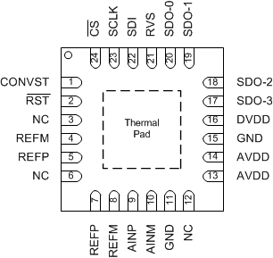
5 Pin Configuration and Functions
RGE Package
24-Pin VQFN
Top View

Pin Functions
| PIN | FUNCTION | DESCRIPTION | |
|---|---|---|---|
| NAME | NO. | ||
| AINM | 10 | Analog input | Negative analog input |
| AINP | 9 | Analog input | Positive analog input |
| AVDD | 13, 14 | Power supply | Analog power supply for the device |
| CONVST | 1 | Digital input | Conversion start input pin for the device. A CONVST rising edge brings the device from ACQ state to CNV state. |
| CS | 24 | Digital input | Chip-select input pin for the device; active low. The device takes control of the data bus when CS is low. The SDO-x pins go to tri-state when CS is high. |
| DVDD | 16 | Power supply | Interface supply |
| GND | 11, 15 | Power supply | Ground |
| NC | 3, 6, 12 | No connection | These pins must be left floating with no external connection |
| REFM | 4, 8 | Analog input | Reference ground potential |
| REFP | 5, 7 | Analog input | Reference voltage input |
| RST | 2 | Digital input | Asynchronous reset input pin for the device. A low pulse on the RST pin resets the device and all register bits return to a default state. |
| RVS | 21 | Digital output | Multi-function output pin for the device. With CS held high, RVS reflects the status of the internal ADCST signal. With CS low, the status of RVS depends on the output protocol selection. |
| SCLK | 23 | Digital input | Clock input pin for the serial interface. All system-synchronous data transfer protocols are timed with respect to the SCLK signal. |
| SDI | 22 | Digital input | Serial data input pin for the device. This pin is used to feed the data or command into the device. |
| SDO-0 | 20 | Digital output | Serial communication: data output 0 |
| SDO-1 | 19 | Digital output | Serial communication: data output 1 |
| SDO-2 | 18 | Digital output | Serial communication: data output 2 |
| SDO-3 | 17 | Digital output | Serial communication: data output 3 |
| Thermal pad | Supply | Exposed thermal pad; connecting this pin to GND is recommended | |