JAJSCI8 September 2016 ISO5452-Q1
PRODUCTION DATA.
- 1 特長
- 2 アプリケーション
- 3 概要
- 4 改訂履歴
- 5 概要(続き)
- 6 Pin Configuration and Function
-
7 Specifications
- 7.1 Absolute Maximum Ratings
- 7.2 ESD Ratings
- 7.3 Recommended Operating Conditions
- 7.4 Thermal Information
- 7.5 Power Rating
- 7.6 Insulation Characteristics
- 7.7 Safety Limiting Values
- 7.8 Safety-Related Certifications
- 7.9 Electrical Characteristics
- 7.10 Switching Characteristics
- 7.11 Safety and Insulation Characteristics Curves
- 7.12 Typical Characteristics
- 8 Parameter Measurement Information
- 9 Detailed Description
-
10Application and Implementation
- 10.1 Application Information
- 10.2
Typical Applications
- 10.2.1 Design Requirements
- 10.2.2
Detailed Design Procedure
- 10.2.2.1 Recommended ISO5452-Q1 Application Circuit
- 10.2.2.2 FLT and RDY Pin Circuitry
- 10.2.2.3 Driving the Control Inputs
- 10.2.2.4 Local Shutdown and Reset
- 10.2.2.5 Global-Shutdown and Reset
- 10.2.2.6 Auto-Reset
- 10.2.2.7 DESAT Pin Protection
- 10.2.2.8 DESAT Diode and DESAT Threshold
- 10.2.2.9 Determining the Maximum Available, Dynamic Output Power, POD-max
- 10.2.2.10 Example
- 10.2.2.11 Higher Output Current Using an External Current Buffer
- 10.2.3 Application Curve
- 11Power Supply Recommendations
- 12Layout
- 13デバイスおよびドキュメントのサポート
- 14メカニカル、パッケージ、および注文情報
8 Parameter Measurement Information
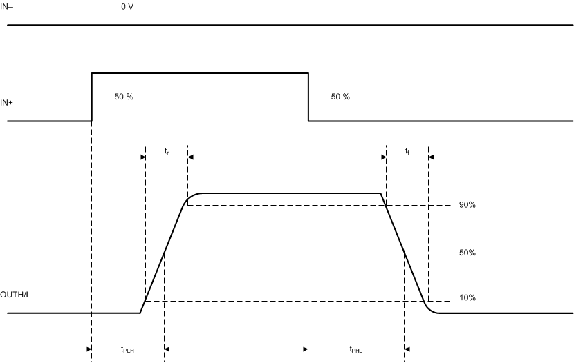
 Figure 44. OUTH/L Propagation Delay, Non-Inverting Configuration
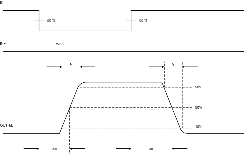
 Figure 45. OUTH/L Propagation Delay, Inverting Configuration
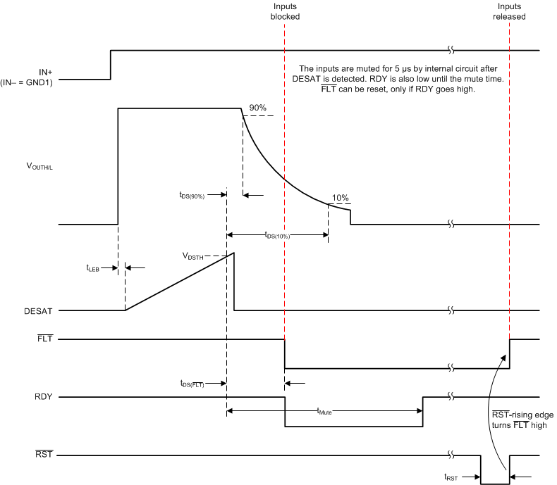
 Figure 46. DESAT, OUTH/L, FLT, RST Delay
 Figure 47. Common-Mode Transient Immunity Test Circuit