JAJSCL6A November 2016 – January 2022 UCC20520
PRODUCTION DATA
- 1 特長
- 2 アプリケーション
- 3 概要
- 4 Revision History
- 5 Pin Configuration and Functions
-
6 Specifications
- 6.1 Absolute Maximum Ratings
- 6.2 ESD Ratings
- 6.3 Recommended Operating Conditions
- 6.4 Thermal Information
- 6.5 Power Ratings
- 6.6 Insulation Specifications
- 6.7 Safety-Related Certifications
- 6.8 Safety-Limiting Values
- 6.9 Electrical Characteristics
- 6.10 Switching Characteristics
- 6.11 Insulation Characteristics Curves
- 6.12 Typical Characteristics
- 7 Parameter Measurement Information
- 8 Detailed Description
-
9 Application and Implementation
- 9.1 Application Information
- 9.2
Typical Application
- 9.2.1 Design Requirements
- 9.2.2
Detailed Design Procedure
- 9.2.2.1 Designing PWM Input Filter
- 9.2.2.2 Select External Bootstrap Diode and its Series Resistor
- 9.2.2.3 Gate Driver Output Resistor
- 9.2.2.4 Estimate Gate Driver Power Loss
- 9.2.2.5 Estimating Junction Temperature
- 9.2.2.6 Selecting VCCI, VDDA/B Capacitor
- 9.2.2.7 Dead Time Setting Guidelines
- 9.2.2.8 Application Circuits with Output Stage Negative Bias
- 9.2.2.9 56
- 9.2.3 Application Curves
- 10Layout
- 11Device and Documentation Support
6.11 Insulation Characteristics Curves
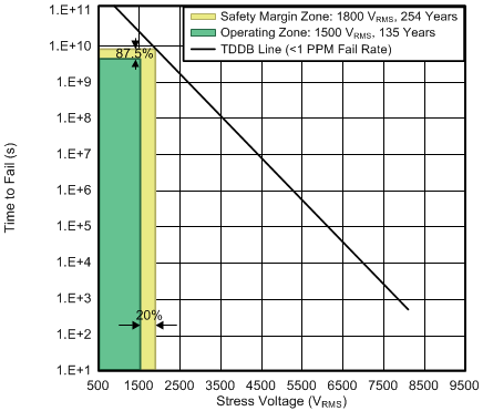
 Figure 6-1 Reinforced Isolation Capacitor Life Time Projection
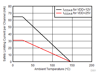
 Figure 6-2 Thermal Derating Curve for Safety-Related Limiting Current (Current in Each Channel with Both Channels Running Simultaneously)
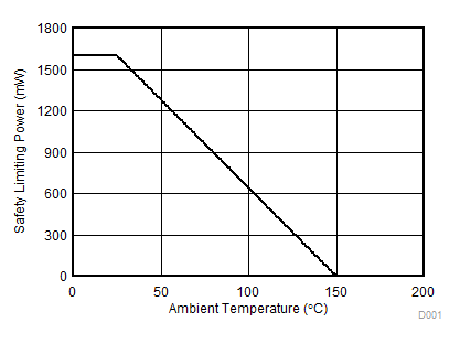
 Figure 6-3 Thermal Derating Curve for Safety-Related Limiting Power