JAJSCO4D November   2016  – December 2023 TPS22976

PRODUCTION DATA  

  1.   1
  2. 特長
  3. アプリケーション
  4. 概要
  5. Device Comparison Table
  6. Pin Configuration and Functions
    1.     Pin Functions
  7. Specifications
    1. 6.1  Absolute Maximum Ratings
    2. 6.2  ESD Ratings
    3. 6.3  Recommended Operating Conditions
    4. 6.4  Thermal Information
    5. 6.5  Electrical Characteristics (VBIAS = 5V)
    6. 6.6  Electrical Characteristics (VBIAS = 2.5V)
    7. 6.7  Switching Characteristics (TPS22976)
    8. 6.8  Switching Characteristics (TPS22976A)
    9. 6.9  Switching Characteristics (TPS22976N)
    10. 6.10 Typical DC Characteristics
    11. 6.11 Typical AC Characteristics
  8. Parameter Measurement Information
  9. Detailed Description
    1. 8.1 Overview
    2. 8.2 Functional Block Diagram
    3. 8.3 Feature Description
      1. 8.3.1 ON and OFF Control
      2. 8.3.2 Input Capacitor (Optional)
      3. 8.3.3 Output Capacitor (Optional)
      4. 8.3.4 Quick Output Discharge (QOD) (Not Present in TPS22976N)
      5. 8.3.5 Thermal Shutdown
    4. 8.4 Device Functional Modes
  10. Application and Implementation
    1. 9.1 Application Information
      1. 9.1.1 Parallel Configuration
      2. 9.1.2 Standby Power Reduction
      3. 9.1.3 Power Supply Sequencing without GPIO Input
      4. 9.1.4 Reverse Current Blocking
    2. 9.2 Typical Application
      1. 9.2.1 Design Requirements
      2. 9.2.2 Detailed Design Procedure
        1. 9.2.2.1 Inrush Current
        2. 9.2.2.2 Adjustable Rise Time
      3. 9.2.3 Application Curves
    3. 9.3 Power Supply Recommendations
    4. 9.4 Layout
      1. 9.4.1 Layout Guidelines
      2. 9.4.2 Layout Example
      3. 9.4.3 Power Dissipation
  11. 10Device and Documentation Support
    1. 10.1 Device Support
      1. 10.1.1 Developmental Support
    2. 10.2 Documentation Support
      1. 10.2.1 Related Documentation
    3. 10.3 ドキュメントの更新通知を受け取る方法
    4. 10.4 サポート・リソース
    5. 10.5 Trademarks
    6. 10.6 静電気放電に関する注意事項
    7. 10.7 用語集
  12. 11Revision History
  13. 12Mechanical, Packaging, and Orderable Information

Reverse Current Blocking

Reverse current blocking is often desired in specific applications, as it prevents current from flowing from the output to the input of the load switch when the device is disabled. With the configuration illustrated in Figure 9-4, the TPS22976 can be converted into a single-channel switch with reverse current blocking. VIN1 or VIN2 can be used as the input and VIN2 or VIN1 as the output.
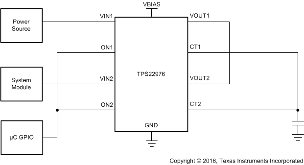
GUID-F022AC46-EBF8-4566-8E20-642AC2B73B67-low.gifFigure 9-4 Reverse Current Blocking