JAJSCS0C December   2016  – January 2018 TPS22810

PRODUCTION DATA.  

  1. 特長
  2. アプリケーション
  3. 概要
    1.     概略回路図
  4. 改訂履歴
  5. Device Comparison Table
  6. Pin Configuration and Functions
    1.     Pin Functions
  7. Specifications
    1. 7.1 Absolute Maximum Ratings
    2. 7.2 ESD Ratings
    3. 7.3 Recommended Operating Conditions
    4. 7.4 Thermal Information
    5. 7.5 Electrical Characteristics
    6. 7.6 Switching Characteristics
    7. 7.7 Typical DC Characteristics
    8. 7.8 Typical AC Characteristics
  8. Parameter Measurement Information
  9. Detailed Description
    1. 9.1 Overview
    2. 9.2 Functional Block Diagram
    3. 9.3 Feature Description
      1. 9.3.1 On and Off Control
      2. 9.3.2 Quick Output Discharge (QOD)
        1. 9.3.2.1 QOD when System Power is Removed
        2. 9.3.2.2 Internal QOD Considerations
      3. 9.3.3 EN/UVLO
      4. 9.3.4 Adjustable Rise Time (CT)
      5. 9.3.5 Thermal Shutdown
    4. 9.4 Device Functional Modes
  10. 10Application and Implementation
    1. 10.1 Application Information
    2. 10.2 ON and OFF Control
    3. 10.3 Input Capacitor (Optional)
    4. 10.4 Output Capacitor (Optional)
    5. 10.5 Typical Application
      1. 10.5.1 Design Requirements
      2. 10.5.2 Detailed Design Procedure
        1. 10.5.2.1 Shutdown Sequencing During Unexpected Power Loss
        2. 10.5.2.2 VIN to VOUT Voltage Drop
        3. 10.5.2.3 Inrush Current
      3. 10.5.3 Application Curves
  11. 11Power Supply Recommendations
  12. 12Layout
    1. 12.1 Layout Guidelines
    2. 12.2 Layout Example
    3. 12.3 Thermal Considerations
  13. 13デバイスおよびドキュメントのサポート
    1. 13.1 デバイス・サポート
      1. 13.1.1 開発サポート
    2. 13.2 ドキュメントのサポート
      1. 13.2.1 関連資料
    3. 13.3 ドキュメントの更新通知を受け取る方法
    4. 13.4 コミュニティ・リソース
    5. 13.5 商標
    6. 13.6 静電気放電に関する注意事項
    7. 13.7 Glossary
  14. 14メカニカル、パッケージ、および注文情報

Application Curves

See the oscilloscope captures below for an example of how the CT capacitor can be used to reduce inrush current for VIN = 12 V. See the Adjustable Rise Time (CT) section for rise times for corresponding CT values.
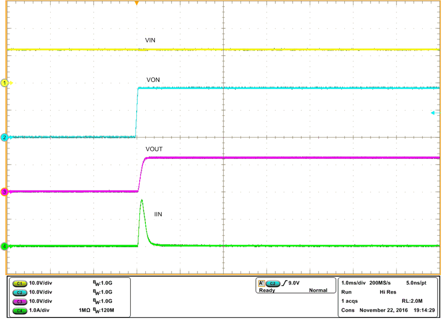
TPS22810 tps22810_Fig35_VIN_12V_CT_0pF_CIN_1.gif
Figure 28. TPS22810 Inrush Current With
CL = 22 µF, CT = 0 pF
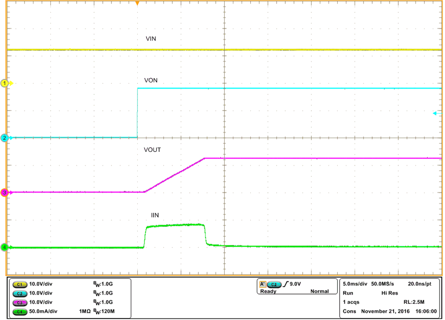
TPS22810 tps22810_Fig37_VIN_12V_CT_27000pF_C.gif
Figure 30. TPS22810 Inrush Current
With CL = 22 µF, CT = 27000 pF
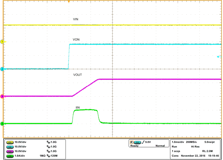
TPS22810 tps22810_Fig39_VIN_12V_CT_4700pF_CI.gif
Figure 32. TPS22810 Inrush Current
With CL = 100 µF, CT = 4700 pF
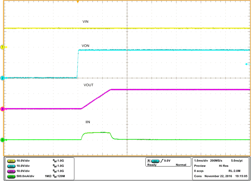
TPS22810 tps22810_Fig36_VIN_12V_CT_4700pF_CI.gif
Figure 29. TPS22810 Inrush Current
with CL = 22 µF, CT = 4700 pF
TPS22810 tps22810_Fig38_VIN_12V_CT_0pF_COUT_.gif
Figure 31. TPS22810 Inrush Current
With CL = 100 µF, CT = 0 pF
TPS22810 tps22810_Fig38_VIN_12V_CT_27000pF_C.gif
Figure 33. TPS22810 Inrush Current
With CL = 100 µF, CT = 27000 pF