JAJSCV6B December 2016 – June 2017 LM5166
PRODUCTION DATA.
- 1 特長
- 2 アプリケーション
- 3 概要
- 4 改訂履歴
- 5 Pin Configuration and Functions
- 6 Specifications
-
7 Detailed Description
- 7.1 Overview
- 7.2 Functional Block Diagram
- 7.3
Feature Description
- 7.3.1 Integrated Power MOSFETs
- 7.3.2 Selectable PFM or COT Mode Converter Operation
- 7.3.3 Low Dropout Operation and 100% Duty Cycle Mode
- 7.3.4 Adjustable Output Voltage (FB)
- 7.3.5 Adjustable Current Limit
- 7.3.6 Precision Enable (EN) and Hysteresis (HYS)
- 7.3.7 Power Good (PGOOD)
- 7.3.8 Configurable Soft Start (SS)
- 7.3.9 Short-Circuit Operation
- 7.3.10 Thermal Shutdown
- 7.4 Device Functional Modes
-
8 Applications and Implementation
- 8.1 Application Information
- 8.2
Typical Applications
- 8.2.1
Design 1: Wide VIN, Low IQ, High-Efficiency COT Converter Rated at 5 V, 500 mA
- 8.2.1.1 Design Requirements
- 8.2.1.2
Detailed Design Procedure
- 8.2.1.2.1 Custom Design With WEBENCH® Tools
- 8.2.1.2.2 Feedback Resistors - RFB1, RFB2
- 8.2.1.2.3 Switching Frequency - RT
- 8.2.1.2.4 Filter Inductance - LF
- 8.2.1.2.5 Output Capacitors - COUT
- 8.2.1.2.6 Ripple Generation Network - RESR, CFF
- 8.2.1.2.7 Input Capacitor - CIN
- 8.2.1.2.8 Soft-Start Capacitor - CSS
- 8.2.1.2.9 Application Curves
- 8.2.2 Design 2: Wide VIN, Low IQ COT Converter Rated at 3.3 V, 500 mA
- 8.2.3 Design 3: High-Density PFM Converter Rated at 3.3 V, 0.3 A
- 8.2.4 Design 4: Wide VIN, Low IQ PFM Converter Rated at 5 V, 500 mA
- 8.2.5
Design 5: 12-V, 300-mA COT Converter Operating From 24-V or 48-V Input
- 8.2.5.1 Design Requirements
- 8.2.5.2
Detailed Design Procedure
- 8.2.5.2.1 Peak Current Limit Setting - RILIM
- 8.2.5.2.2 Switching Frequency - RRT
- 8.2.5.2.3 Inductor - LF
- 8.2.5.2.4 Input and Output Capacitors - CIN, COUT
- 8.2.5.2.5 Feedback Resistors - RFB1, RFB2
- 8.2.5.2.6 Ripple Generation Network - RA, CA, CB
- 8.2.5.2.7 Undervoltage Lockout Setpoint - RUV1, RUV2, RHYS
- 8.2.5.2.8 Soft Start - CSS
- 8.2.5.3 Application Curves
- 8.2.1
Design 1: Wide VIN, Low IQ, High-Efficiency COT Converter Rated at 5 V, 500 mA
- 9 Power Supply Recommendations
- 10Layout
- 11デバイスおよびドキュメントのサポート
- 12メカニカル、パッケージ、および注文情報
10 Layout
The performance of any switching converter depends as much upon PCB layout as it does the component selection. The following guidelines are provided to assist with designing a PCB with the best power conversion performance, thermal performance, and minimized generation of unwanted EMI.
10.1 Layout Guidelines
PCB layout is a critical portion of good power supply design. There are several paths that conduct high slew-rate currents or voltages that can interact with stray inductance or parasitic capacitance to generate noise and EMI or degrade the power supply performance.
- To help eliminate these problems, bypass the VIN pin to GND with a low-ESR ceramic bypass capacitor with a high-quality dielectric. Place CIN as close as possible to the LM5166 VIN and GND pins. Grounding for both the input and output capacitors should consist of localized top-side planes that connect to the GND pin and GND PAD.
- Minimize the loop area formed by the input capacitor connections to the VIN and GND pins.
- Locate the inductor close to the SW pin. Minimize the area of the SW trace or plane to prevent excessive capacitive coupling.
- Tie the GND pin directly to the power pad under the device and to a heat-sinking PCB ground plane.
- Use a ground plane in one of the middle layers as noise shielding and heat dissipation path.
- Have a single-point ground connection to the plane. Route the ground connections for the feedback, soft-start, and enable components to the ground plane. This prevents any switched or load currents from flowing in analog ground traces. If not properly handled, poor grounding results in degraded load regulation or erratic output voltage ripple behavior.
- Make VIN, VOUT and ground bus connections as wide as possible. This reduces any voltage drops on the input or output paths of the converter and maximizes efficiency.
- Minimize trace length to the FB pin. Place both feedback resistors, RFB1 and RFB2, close to the FB pin. Place CFF (if needed) directly in parallel with RFB1. If output setpoint accuracy at the load is important, connect the VOUT sense at the load. Route the VOUT sense path away from noisy nodes and preferably through a layer on the other side of a shielding layer.
- The RT pin is sensitive to noise. Thus, locate the RRT resistor as close as possible to the device and route with minimal lengths of trace. The parasitic capacitance from RT to GND must not exceed 20 pF.
- Provide adequate heat sinking for the LM5166 to keep the junction temperature below 150°C. For operation at full rated load, the top-side ground plane is an important heat-dissipating area. Use an array of heat-sinking vias to connect the exposed pad to the PCB ground plane. If the PCB has multiple copper layers, these thermal vias must also be connected to inner layer heat-spreading ground planes.
10.1.1 Compact PCB Layout for EMI Reduction
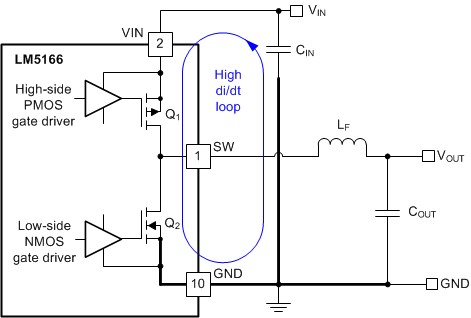
Radiated EMI generated by high di/dt components relates to pulsing currents in switching converters. The larger area covered by the path of a pulsing current, the more electromagnetic emission is generated. The key to minimizing radiated EMI is to identify the pulsing current path and minimize the area of that path.
The critical switching loop of the buck converter power stage in terms of EMI is denoted in Figure 89. The topological architecture of a buck converter means that a particularly high di/dt current path exists in the loop comprising the input capacitor and the integrated MOSFETs of the LM5166, and it becomes mandatory to reduce the parasitic inductance of this loop by minimizing the effective loop area.
 Figure 89. DC-DC Buck Converter With Power Stage Circuit Switching Loops
The input capacitor provides the primary path for the high di/dt components of the high-side MOSFET's current. Placing a ceramic capacitor as close as possible to the VIN and GND pins is the key to EMI reduction. Keep the trace connecting SW to the inductor as short as possible and just wide enough to carry the load current without excessive heating. Use short, thick traces or copper pours (shapes) for current conduction path to minimize parasitic resistance. Place the output capacitor close to the VOUT side of the inductor, and connect the capacitor's return terminal to the GND pin and exposed PAD of the LM5166.
10.1.2 Feedback Resistors
For the adjustable output voltage version of the LM5166, reduce noise sensitivity of the output voltage feedback path by placing the resistor divider close to the FB pin, rather than close to the load. This reduces the trace length of FB signal and noise coupling. The FB pin is the input to the feedback comparator, and as such is a high impedance node sensitive to noise. The output node is a low impedance node, so the trace from VOUT to the resistor divider can be long if a short path is not available.
Route the voltage sense trace from the load to the feedback resistor divider, keeping away from the SW node, the inductor and VIN to avoid contaminating the feedback signal with switch noise, while also minimizing the trace length. This is most important when high feedback resistances, greater than 100 kΩ, are used to set the output voltage. Also, route the voltage sense trace on a different layer from the inductor, SW node and VIN, such that there is a ground plane that separates the feedback trace from the inductor and SW node copper polygon. This provides further shielding for the voltage feedback path from switching noise sources
10.2 Layout Example
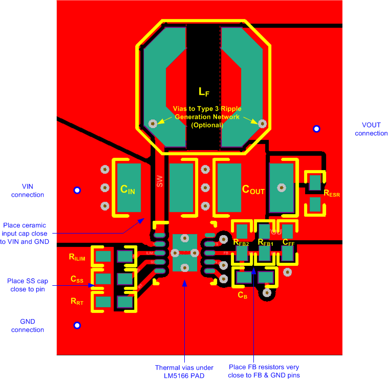
Figure 90 shows an example layout for the PCB top layer of a 4-layer board with essential components placed on the top side. The bottom layer features optional Type 3 ripple generation components (RA and CA), and RUV1, RUV2, and RHYS resistors.
 Figure 90. LM5166 Single-Sided PCB Layout Example