JAJSCV7E august   2016  – november 2020 DS90UB933-Q1

PRODUCTION DATA  

  1.   1
  2. 特長
  3. アプリケーション
  4. 概要
  5. Revision History
  6. Pin Configuration and Functions
    1.     Pin Functions
  7. Specifications
    1. 6.1  Absolute Maximum Ratings
    2. 6.2  ESD Ratings
    3. 6.3  Recommended Operating Conditions
    4. 6.4  Thermal Information
    5. 6.5  Electrical Characteristics
    6. 6.6  Recommended Serializer Timing For PCLK
    7. 6.7  AC Timing Specifications (SCL, SDA) - I2C-Compatible
    8. 6.8  Bidirectional Control Bus DC Timing Specifications (SCL, SDA) - I2C-Compatible
    9. 6.9  Serializer Switching Characteristics
    10. 6.10 Timing Diagrams
    11. 6.11 Typical Characteristics
  8. Detailed Description
    1. 7.1 Overview
    2. 7.2 Functional Block Diagram
    3. 7.3 Feature Description
      1. 7.3.1 Serial Frame Format
      2. 7.3.2 Line Rate Calculations for the DS90UB933/934
      3. 7.3.3 Error Detection
      4. 7.3.4 Synchronizing Multiple Cameras
      5. 7.3.5 General Purpose I/O (GPIO) Descriptions
      6. 7.3.6 LVCMOS V(VDDIO) Option
      7. 7.3.7 Pixel Clock Edge Select (TRFB / RRFB)
      8. 7.3.8 Power Down
    4. 7.4 Device Functional Modes
      1. 7.4.1 DS90UB933/934 Operation With External Oscillator as Reference Clock
      2. 7.4.2 DS90UB933/934 Operation With Pixel Clock From Imager as Reference Clock
      3. 7.4.3 MODE Pin on Serializer
      4. 7.4.4 Internal Oscillator
      5. 7.4.5 Built-In Self Test
      6. 7.4.6 BIST Configuration and Status
      7. 7.4.7 Sample BIST Sequence
    5. 7.5 Programming
      1. 7.5.1 Programmable Controller
      2. 7.5.2 Description of Bidirectional Control Bus and I2C Modes
      3. 7.5.3 I2C Pass-Through
      4. 7.5.4 Slave Clock Stretching
      5. 7.5.5 IDX Address Decoder on the Serializer
      6. 7.5.6 Multiple Device Addressing
    6. 7.6 Register Maps
  9. Application and Implementation
    1. 8.1 Application Information
      1. 8.1.1 Power Over Coax
      2. 8.1.2 Power-Up Requirements and PDB Pin
      3. 8.1.3 AC Coupling
      4. 8.1.4 Transmission Media
    2. 8.2 Typical Applications
      1. 8.2.1 Coax Application
        1. 8.2.1.1 Design Requirements
        2. 8.2.1.2 Detailed Design Procedure
        3. 8.2.1.3 Application Curves
      2. 8.2.2 STP Application
        1. 8.2.2.1 Design Requirements
        2. 8.2.2.2 Detailed Design Procedure
        3. 8.2.2.3 62
  10. Power Supply Recommendations
  11. 10Layout
    1. 10.1 Layout Guidelines
      1. 10.1.1 Interconnect Guidelines
    2. 10.2 Layout Example
  12. 11Device and Documentation Support
    1. 11.1 Documentation Support
      1. 11.1.1 Related Documentation
    2. 11.2 Receiving Notification of Documentation Updates
    3. 11.3 サポート・リソース
    4. 11.4 Trademarks
    5. 11.5 静電気放電に関する注意事項
    6. 11.6 用語集

MODE Pin on Serializer

The MODE pin on the serializer can be configured to select if the DS90UB933-Q1 device is to be operated from the external oscillator or the PCLK from the imager. The pin must be pulled to VDD_n(1.8 V, not VDDIO) with a resistor R1 and a pulldown resistor R2 for external oscillator mode to create the ratio shown in Figure 7-6. If the device is to be operated from PCLK from imager mode, MODE pin can be pulled up to VDD_n (1.8V) with a 10-kΩ resistor directly or use the ratio shown in Figure 7-6 and Table 7-2. Suggested resistor values are given in Table 7-2. The recommended maximum resistor tolerance is 1%. Other resistor values can be used as long as the ratio is met under all conditions.
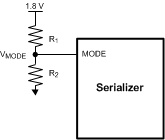
GUID-FFABAACF-DEE7-4AB5-8FE6-1048E9BEFB47-low.gifFigure 7-6 MODE Pin Configuration on DS90UB933-Q1
Table 7-2 DS90UB933-Q1 Serializer
MODE Setting
DS90UB933-Q1 SERIALIZER MODE SETTING
MODE SELECTMINIMUM RATIO (VMODE/V(VDD_n))MAXIMUM RATIO (VMODE/V(VDD_n))SUGGESTED R1 RESISTOR VALUE (kΩ)SUGGESTED R2 RESISTOR VALUE (kΩ)
PCLK from imager mode0.7501.0001050
External oscillator mode0.2920.339104.7