JAJSD07C September 2016 – December 2022 DS90UB934-Q1
PRODUCTION DATA
- 特長
- 1アプリケーション
- 2概要
- 3Revision History
- Pin Configuration and Functions
- 4Specifications
-
5Detailed Description
- 5.1 Overview
- 5.2 Functional Block Diagram
- 5.3 Feature Description
- 5.4 Device Functional Modes
- 5.5 Programming
- 5.6 Register Maps
- 6Application and Implementation
- Mechanical, Packaging, and Orderable Information
- 7Device and Documentation Support
- Mechanical, Packaging, and Orderable Information
6.2 Power Over Coax
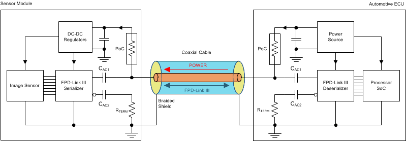
The DS90UB34-Q1 is designed to support the Power-over-Coax (PoC) method of powering remote sensor systems. With this method, the power is delivered over the same medium (a coaxial cable) used for high-speed digital video data and bidirectional control and diagnostics data transmission. The method utilizes passive networks or filters that isolate the transmission line from the loading of the DC-DC regulator circuits and their connecting power traces on both sides of the link as shown in Figure 6-1.
 Figure 6-1 Power Over Coax (PoC) System Diagram
The PoC networks' impedance of ≥ 2 kΩ over a specific frequency band is typically sufficient to isolate the transmission line from the loading of the regulator circuits. The lower limit of the frequency band is defined as ½ of the frequency of the bidirectional control channel, fBCC. The upper limit of the frequency band is the frequency of the forward high-speed channel, fFC.
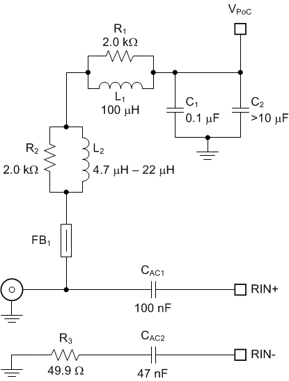
Figure 6-2 shows a PoC network recommended for a FPD-Link III consisting of DS90UB913A-Q1/DS90UB933-Q1 and DS90UB934-Q1 pair with the bidirectional channel operating at 5 Mbps (½ fBCC = 2.5 MHz) and the forward channel operating at 1.87 Gbps (fFC = 1GHz).
 Figure 6-2 Typical PoC Network for a 2G FPD-Link III
Table 6-1 lists essential components for this particular PoC network.
| COUNT | REF DES | DESCRIPTION | PART NUMBER | MFR |
|---|---|---|---|---|
| 1 | L1 | Inductor, 100 µH, 0.310 Ω maximum, 710 mA minimum (Isat, Itemp) 7.2-MHz SRF typical, 6.6 mm × 6.6 mm, AEC-Q200 | MSS7341-104ML | Coilcraft |
| 1 | L2 | Inductor, 4.7 µH, 0.350 Ω maximum, 700 mA minimum (Isat, Itemp) 160-MHz SRF typical, 3.8 mm x 3.8 mm, AEC-Q200 | 1008PS-472KL | Coilcraft |
| Inductor, 4.7 µH, 0.130 Ω maximum, 830 mA minimum (Isat, Itemp), 70-MHz SRF typical, 3.2 mm × 2.5 mm, AEC-Q200 | CBC3225T4R7MRV | Taiyo Yuden | ||
| 1 | FB1 | Ferrite Bead, 1500 kΩ at 1 GHz, 0.5 Ω maximum at DC 500-mA at 85°C, SM0603, General-Purpose | BLM18HE152SN1 | Murata |
| Ferrite Bead, 1500 kΩ at 1 GHz, 0.5 Ω maximum at DC 500-mA at 85°C, SM0603, AEC-Q200 | BLM18HE152SZ1 | Murata |
Application report Sending Power over Coax in DS90UB913A Designs (SNLA224) discusses defining PoC networks in more detail.
In addition to the PoC network components selection, their placement and layout play a critical role as well.
- Place the smallest component, typically a ferrite bead or a chip inductor, as close to the connector as possible. Route the high-speed trace through one of its pads to avoid stubs.
- Use the smallest component pads as allowed by manufacturer's design rules. Add anti-pads in the inner planes below the component pads to minimize impedance drop.
- Consult with connector manufacturer for optimized connector footprint. If the connector is mounted on the same side as the IC, minimize the impact of the thru-hole connector stubs by routing the high-speed signal traces on the opposite side of the connector mounting side.
- Use coupled 100-Ω differential signal traces from the device pins to the AC-coupling caps. Use 50-Ω single-ended traces from the AC-coupling capacitors to the connector.
- Terminate the inverting signal traces close to the connectors with standard 49.9-Ω resistors.
The suggested characteristics for single-ended PCB traces (microstrips or striplines) for serializer or deserializer boards are detailed in Table 6-2. The effects of the PoC networks need to be accounted for when testing the traces for compliance to the suggested limits.
| PARAMETER | MIN | TYP | MAX | UNIT | ||
|---|---|---|---|---|---|---|
| Ltrace | Single-ended PCB trace length from the device pin to the connector pin | 5 | cm | |||
| Ztrace | Single-ended PCB trace characteristic impedance | 45 | 50 | 55 | Ω | |
| Zcon | Connector (mounted) characteristic impedance | 40 | 50 | 60 | Ω | |
| RL | Return Loss, S11 | ½ fBCC < f < 0.1 GHz | –20 | dB | ||
| 0.1 GHz < f < 1 GHz (f in GHz) | –12+8*log(f) | dB | ||||
| IL | Insertion Loss, S12 | f <0.5 GHz | -0.35 | dB | ||
| f=1 GHz | –0.6 | dB | ||||
The VPOC noise needs to be kept to 10 mVp-p or lower on the source / deserializer side of the system. The VPOC fluctuations on the serializer side, caused by the transient current draw of the sensor and the DC resistance of cables and PoC components, need to be kept at minimum as well. Increasing the VPOC voltage and adding extra decoupling capacitance (> 10 µF) help reduce the amplitude and slew rate of the VPOC fluctuations.