JAJSD07C September 2016 – December 2022 DS90UB934-Q1
PRODUCTION DATA
- 特長
- 1アプリケーション
- 2概要
- 3Revision History
- Pin Configuration and Functions
- 4Specifications
-
5Detailed Description
- 5.1 Overview
- 5.2 Functional Block Diagram
- 5.3 Feature Description
- 5.4 Device Functional Modes
- 5.5 Programming
- 5.6 Register Maps
- 6Application and Implementation
- Mechanical, Packaging, and Orderable Information
- 7Device and Documentation Support
- Mechanical, Packaging, and Orderable Information
5.5.1 Serial Control Bus
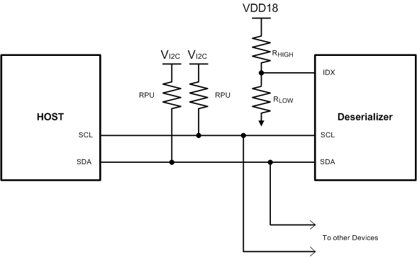
The DS90UB934-Q1 implements an I2C-compatible serial control bus. The I2C is for local device configuration and incorporates a bidirectional control channel (BCC) that allows communication with a remote serializers as well as remote I2C target devices.
The device address is set via a resistor divider (RHIGH and RLOW — see Figure 5-6) connected to the IDX pin.
 Figure 5-6 Serial Control Bus Connection
The serial control bus consists of two signals, SCL and SDA. SCL is a serial bus clock input. SDA is the serial bus data input/output signal. Both SCL and SDA signals require an external pullup resistor to 1.8-V or 3.3-V V(VI2C). The pullup resistor value may be adjusted for capacitive loading and data rate requirements. The signals are either pulled high or driven low.
The IDX pin configures the control interface to one of 8 possible device addresses. A pullup resistor and a pulldown resistor may be used to set the appropriate voltage ratio between the IDX input pin (V(IDX)) and V(VI2C), each ratio corresponding to a specific device address (see Table 5-7).
| VIDX VOLTAGE RANGE | VIDX TARGET VOLTAGE | SUGGESTED STRAP RESISTORS (1% TOL) | ASSIGNED I2C ADDRESS | |||||
|---|---|---|---|---|---|---|---|---|
| NO. | VMIN | VTYP | VMAX | (V); V(VDD18) = 1.8 V | RHIGH (kΩ ) | RLOW (kΩ ) | 7-BIT | 8-BIT |
| 0 | 0 | 0 | 0.131 × V(VDD18) | 0 | OPEN | 10.0 | 0x30 | 0x60 |
| 1 | 0.179 × V(VDD18) | 0.213 × V(VDD18) | 0.247 × V(VDD18) | 0.374 | 88.7 | 23.2 | 0x32 | 0x64 |
| 2 | 0.296 × V(VDD18) | 0.330 × V(VDD18) | 0.362 × V(VDD18) | 0.582 | 75.0 | 35.7 | 0x34 | 0x68 |
| 3 | 0.412 × V(VDD18) | 0.443 × V(VDD18) | 0.474 × V(VDD18) | 0.792 | 71.5 | 56.2 | 0x36 | 0x6C |
| 4 | 0.525 × V(VDD18) | 0.559 × V(VDD18) | 0.592 × V(VDD18) | 0.995 | 78.7 | 97.6 | 0x38 | 0x70 |
| 5 | 0.642 × V(VDD18) | 0.673 × V(VDD18) | 0.704 × V(VDD18) | 1.202 | 39.2 | 78.7 | 0x3A | 0x74 |
| 6 | 0.761 × V(VDD18) | 0.792 × V(VDD18) | 0.823 × V(VDD18) | 1.420 | 25.5 | 95.3 | 0x3C | 0x78 |
| 7 | 0.876 × V(VDD18) | V(VDD18) | V(VDD18) | 1.8 | 10 | OPEN | 0x3D | 0x7A |
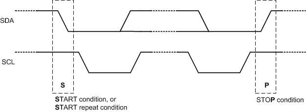
The serial bus protocol is controlled by START, START-Repeated, and STOP phases. A START occurs when SDA transitions low while SCL is high. A STOP occurs when SDA transitions high while SCL is also high. See Figure 5-7.
 Figure 5-7 START and STOP Conditions
To communicate with a remote device, the host controller (controller) sends the target address and listens for a response from the target. This response is referred to as an acknowledge bit (ACK). If a target on the bus is addressed correctly, it acknowledges (ACKs) the controller by driving the SDA bus low. If the address does not match the target address of a device, it not-acknowledges (NACKs) the controller by letting SDA be pulled High. ACKs also occur on the bus when data is being transmitted. When the controller is writing data, the target ACKs after every data byte is successfully received. When the controller is reading data, the controller ACKs after every data byte is received to let the target know it wants to receive another data byte. When the controller wants to stop reading, it NACKs after the last data byte and creates a stop condition on the bus. All communication on the bus begins with either a START condition or a REPEATED-START condition. All communication on the bus ends with a STOP condition. A READ is shown in Figure 5-8 and a WRITE is shown in Figure 5-9.
 Figure 5-8 Serial Control Bus —
READ
 Figure 5-9 Serial Control Bus —
WRITE
 Figure 5-10 Basic Operation
The I2C controller located at the deserializer must support I2C clock stretching. For more information on I2C interface requirements and throughput considerations, refer to AN-2173 I2C Communication Over FPD-Link III with Bidirectional Control Channel (SNLA131).