JAJSDL6D January 2016 – May 2017 TPS61194-Q1
PRODUCTION DATA.
- 1 特長
- 2 アプリケーション
- 3 概要
- 4 改訂履歴
- 5 デバイス比較表
- 6 Pin Configuration and Functions
-
7 Specifications
- 7.1 Absolute Maximum Ratings
- 7.2 ESD Ratings
- 7.3 Recommended Operating Conditions
- 7.4 Thermal Information
- 7.5 Electrical Characteristics
- 7.6 Internal LDO Electrical Characteristics
- 7.7 Protection Electrical Characteristics
- 7.8 Current Sinks Electrical Characteristics
- 7.9 PWM Brightness Control Electrical Characteristics
- 7.10 Boost and SEPIC Converter Characteristics
- 7.11 Logic Interface Characteristics
- 7.12 Typical Characteristics
- 8 Detailed Description
- 9 Application and Implementation
- 10Power Supply Recommendations
- 11Layout
- 12デバイスおよびドキュメントのサポート
- 13メカニカル、パッケージ、および注文情報
7 Specifications
7.1 Absolute Maximum Ratings
Over operating free-air temperature range (unless otherwise noted)(1)(2)| MIN | MAX | UNIT | ||
|---|---|---|---|---|
| Voltage on pins | VIN, SW, FB | –0.3 | 50 | V |
| OUT1, OUT2, OUT3, OUT4 | –0.3 | 45 | ||
| LDO, SYNC, FSET, ISET, PWM, VDDIO/EN, FAULT | –0.3 | 5.5 | ||
| Continuous power dissipation(3) | Internally Limited | |||
| Ambient temperature range TA(4) | –40 | 125 | °C | |
| Junction temperature range TJ(4) | –40 | 150 | °C | |
| Maximum lead temperature (soldering) | See(5) | |||
| Storage temperature, Tstg | –65 | 150 | °C | |
(1) Stresses beyond those listed under absolute maximum ratings may cause permanent damage to the device. These are stress ratings only, and functional operation of the device at these or any other conditions beyond those indicated under recommended operating conditions is not implied. Exposure to absolute-maximum-rated conditions for extended periods may affect device reliability.
(2) All voltages are with respect to the potential at the GND pins.
(3) Internal thermal shutdown circuitry protects the device from permanent damage. Thermal shutdown engages at TJ = 165°C (typical) and disengages at TJ = 145°C (typical).
(4) In applications where high power dissipation and/or poor package thermal resistance is present, the maximum ambient temperature may have to be derated. Maximum ambient temperature (TA-MAX) is dependent on the maximum operating junction temperature (TJ-MAX-OP = 150°C), the maximum power dissipation of the device in the application (PD-MAX), and the junction-to ambient thermal resistance of the part/package in the application (RθJA), as given by the following equation: TA-MAX = TJ-MAX-OP – (RθJA × PD-MAX).
(5) For detailed soldering specifications and information, refer to the PowerPAD™ Thermally Enhanced Package .
7.2 ESD Ratings
| VALUE | UNIT | ||||
|---|---|---|---|---|---|
| V(ESD) | Electrostatic discharge | Human-body model (HBM), per AEC Q100-002(1) | ±2000 | V | |
| Charged-device model (CDM), per AEC Q100-011 | All other pins | ±500 | |||
| Corner pins (1,10,11,20) | ±750 | ||||
(1) AEC Q100-002 indicates that HBM stressing shall be in accordance with the ANSI/ESDA/JEDEC JS-001 specification.
7.3 Recommended Operating Conditions
Over operating free-air temperature range (unless otherwise noted)(1)| MIN | MAX | UNIT | ||
|---|---|---|---|---|
| Voltage on pins | VIN | 4.5 | 45 | V |
| SW | 0 | 45 | ||
| OUT1, OUT2, OUT3, OUT4 | 0 | 40 | ||
| FB, FSET, LDO, ISET, VDDIO/EN, FAULT | 0 | 5.25 | ||
| SYNC, PWM | 0 | VDDIO/EN | ||
(1) All voltages are with respect to the potential at the GND pins.
7.4 Thermal Information
| THERMAL METRIC(1) | TPS61194-Q1 | UNIT | |
|---|---|---|---|
| PWP (HTSSOP) | |||
| 20 PINS | |||
| RθJA | Junction-to-ambient thermal resistance(2) | 44.2 | °C/W |
| RθJCtop | Junction-to-case (top) thermal resistance | 26.5 | °C/W |
| RθJB | Junction-to-board thermal resistance | 22.4 | °C/W |
| ψJT | Junction-to-top characterization parameter | 0.9 | °C/W |
| ψJB | Junction-to-board characterization parameter | 22.2 | °C/W |
| RθJCbot | Junction-to-case (bottom) thermal resistance | 2.5 | °C/W |
(1) For more information about traditional and new thermal metrics, see Semiconductor and IC Package Thermal Metrics.
(2) Junction-to-ambient thermal resistance is highly application and board-layout dependent. In applications where high maximum power dissipation exists, special care must be paid to thermal dissipation issues in board design.
7.5 Electrical Characteristics(1)(2)
TJ = −40°C to +125°C (unless otherwise noted).| PARAMETER | TEST CONDITIONS | MIN | TYP | MAX | UNIT | |
|---|---|---|---|---|---|---|
| IQ | Standby supply current | Device disabled, VVDDIO/EN = 0 V, VIN = 12 V | 4.5 | 20 | μA | |
| Active supply current | VIN = 12 V, VOUT = 26 V, output current 80 mA/channel, converter ƒSW = 300 kHz | 5 | 12 | mA | ||
| VPOR_R | Power-on reset rising threshold | LDO pin voltage | 2.7 | V | ||
| VPOR_F | Power-on reset falling threshold | LDO pin voltage | 1.5 | V | ||
| TTSD | Thermal shutdown threshold | 150 | 165 | 175 | °C | |
| TTSD_HYST | Thermal shutdown hysteresis | 20 | °C | |||
(1) All voltages are with respect to the potential at the GND pins.
(2) Minimum and maximum limits are specified by design, test, or statistical analysis.
7.6 Internal LDO Electrical Characteristics
TJ = −40°C to +125°C (unless otherwise noted).| PARAMETER | TEST CONDITIONS | MIN | TYP | MAX | UNIT | |
|---|---|---|---|---|---|---|
| VLDO | Output voltage | VIN = 12 V | 4.15 | 4.3 | 4.55 | V |
| VDR | Dropout voltage | 120 | 300 | 430 | mV | |
| ISHORT | Short circuit current | 50 | mA | |||
7.7 Protection Electrical Characteristics
TJ = −40°C to +125°C (unless otherwise noted).| PARAMETER | TEST CONDITIONS | MIN | TYP | MAX | UNIT | |
|---|---|---|---|---|---|---|
| VOVP | VIN OVP threshold voltage | 41 | 42 | 44 | V | |
| VUVLO | VIN UVLO | 4 | V | |||
| VUVLO_HYST | VIN UVLO hysteresis | 100 | mV | |||
| LED short detection threshold | 5.6 | 6 | 7 | V | ||
7.8 Current Sinks Electrical Characteristics
TJ = −40°C to +125°C (unless otherwise noted).| PARAMETER | TEST CONDITIONS | MIN | TYP | MAX | UNIT | |
|---|---|---|---|---|---|---|
| ILEAKAGE | Leakage current | Outputs OUT1 to OUT4 , VOUTx = 45 V | 0.1 | 5 | µA | |
| IMAX | Maximum current | OUT1, OUT2, OUT3, OUT4 | 100 | mA | ||
| IOUT | Output current accuracy | IOUT = 100 mA | −5% | 5% | ||
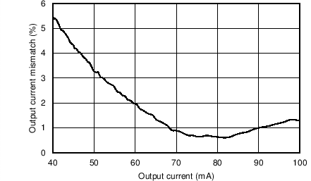
| IMATCH | Output current matching(1) | IOUT = 100 mA, PWM duty =100% | 1% | 5% | ||
| VSAT | Saturation voltage(2) | IOUT = 100 mA | 0.4 | 0.7 | V | |
(1) Output Current Accuracy is the difference between the actual value of the output current and programmed value of this current. Matching is the maximum difference from the average. For the constant current sinks on the part (OUTx), the following are determined: the maximum output current (MAX), the minimum output current (MIN), and the average output current of all outputs (AVG). Matching number is calculated: (MAX-MIN)/AVG. The typical specification provided is the most likely norm of the matching figure for all parts. LED current sinks were characterized with 1-V headroom voltage. Note that some manufacturers have different definitions in use.
(2) Saturation voltage is defined as the voltage when the LED current has dropped 10% from the value measured at 1 V.
7.9 PWM Brightness Control Electrical Characteristics
TJ = −40°C to +125°C (unless otherwise noted).| PARAMETER | TEST CONDITIONS | MIN | TYP | MAX | UNIT | |
|---|---|---|---|---|---|---|
| ƒPWM | PWM input frequency | 100 | 20 000 | Hz | ||
| tON/OFF | Minimum on/off time(1) | 0.5 | µs | |||
7.10 Boost and SEPIC Converter Characteristics
TJ = −40°C to +125°C (unless otherwise noted).Unless otherwise specified: VIN = 12 V, VEN/VDDIO = 3.3 V, L = 22 μH, CIN = 2 × 10-μF ceramic and 33-μF electrolytic,
COUT = 2 × 10-μF ceramic and 33-μF electrolytic, D = NRVB460MFS, ƒSW = 300 kHz.
| PARAMETER | TEST CONDITIONS | MIN | TYP | MAX | UNIT | |
|---|---|---|---|---|---|---|
| VIN | Input voltage | 4.5 | 40 | V | ||
| VOUT | Output voltage | 6 | 45 | |||
| ƒSW_MIN | Minimum switching frequency (central frequency if spread spectrum is enabled) | Defined by RFSET resistor | 300 | kHz | ||
| ƒSW_MAX | Maximum switching frequency (central frequency if spread spectrum is enabled) | 2 200 | kHz | |||
| VOUT/VIN | Conversion ratio | 10 | ||||
| TOFF | Minimum switch OFF time(1) | ƒSW ≥ 1.15 MHz | 55 | ns | ||
| ISW_MAX | SW current limit | 1.8 | 2 | 2.2 | A | |
| RDSON | FET RDSON | Pin-to-pin | 240 | 400 | mΩ | |
| fSYNC | External SYNC frequency | 300 | 2 200 | kHz | ||
| tSYNC_ON_MIN | External SYNC minimum on time(1) | 150 | ns | |||
| tSYNC_OFF_MIN | External SYNC minimum off time(1) | 150 | ns | |||
(1) This specification is not ensured by ATE.
7.11 Logic Interface Characteristics
TJ = −40°C to +125°C (unless otherwise noted).| PARAMETER | TEST CONDITIONS | MIN | TYP | MAX | UNIT | |
|---|---|---|---|---|---|---|
| LOGIC INPUT VDDIO/EN | ||||||
| VIL | Input low level | 0.4 | V | |||
| VIH | Input high level | 1.65 | ||||
| II | Input current | −1 | 5 | 30 | µA | |
| LOGIC INPUT SYNC/FSET, PWM | ||||||
| VIL | Input low level | 0.2 × VDDIO/EN | V | |||
| VIH | Input high level | 0.8 × VDDIO/EN | ||||
| II | Input current | −1 | 1 | μA | ||
| LOGIC OUTPUT FAULT | ||||||
| VOL | Output low level | Pullup current 3 mA | 0.3 | 0.5 | V | |
| ILEAKAGE | Output leakage current | V = 5.5 V | 1 | μA | ||
7.12 Typical Characteristics
Unless otherwise specified: D = NRVB460MFS, T = 25°C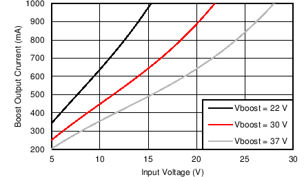
| ƒSW = 300 kHz | L = 33 μH | DC Load (PWM = 100%) |
| CIN and COUT = 33 µF + 2 × 10 µF (ceramic) | ||
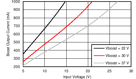
| ƒSW = 1.5 MHz | L = 8.2 μH | DC Load (PWM = 100%) | |
| CIN and COUT = 2 × 10 µF (ceramic) | |||
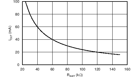

| ƒSW = 800 kHz | L = 15 μH | DC Load (PWM = 100%) |
| CIN and COUT = 2 ×10 µF (ceramic) | ||

| ƒSW = 2.2 MHz | L = 4.7 μH | DC Load (PWM = 100%) |
| CIN and COUT = 2 × 10 µF (ceramic) | ||
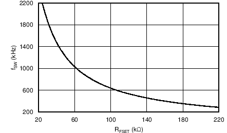
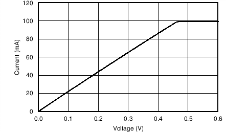
| RISET = 24 kΩ |
