JAJSDO0B May   2017  – October 2018 ADS122U04

PRODUCTION DATA.  

  1. 特長
  2. アプリケーション
  3. 概要
    1.     Device Images
      1.      Kタイプ熱電対温度の測定
  4. 改訂履歴
  5. 概要(続き)
  6. Pin Configuration and Functions
    1.     Pin Functions
  7. Specifications
    1. 7.1 Absolute Maximum Ratings
    2. 7.2 ESD Ratings
    3. 7.3 Recommended Operating Conditions
    4. 7.4 Thermal Information
    5. 7.5 Electrical Characteristics
    6. 7.6 UART Timing Requirements
    7. 7.7 UART Switching Characteristics
    8. 7.8 Typical Characteristics
  8. Parameter Measurement Information
    1. 8.1 Noise Performance
  9. Detailed Description
    1. 9.1 Overview
    2. 9.2 Functional Block Diagram
    3. 9.3 Feature Description
      1. 9.3.1  Multiplexer
      2. 9.3.2  Low-Noise Programmable Gain Stage
        1. 9.3.2.1 PGA Input Voltage Requirements
        2. 9.3.2.2 Bypassing the PGA
      3. 9.3.3  Voltage Reference
      4. 9.3.4  Modulator and Internal Oscillator
      5. 9.3.5  Digital Filter
      6. 9.3.6  Conversion Times
      7. 9.3.7  Excitation Current Sources
      8. 9.3.8  Sensor Detection
      9. 9.3.9  System Monitor
      10. 9.3.10 Temperature Sensor
        1. 9.3.10.1 Converting From Temperature to Digital Codes
          1. 9.3.10.1.1 For Positive Temperatures (For Example, 50°C):
          2. 9.3.10.1.2 For Negative Temperatures (For Example, –25°C):
        2. 9.3.10.2 Converting From Digital Codes to Temperature
      11. 9.3.11 Offset Calibration
      12. 9.3.12 Conversion Data Counter
      13. 9.3.13 Data Integrity
      14. 9.3.14 General-Purpose Digital Inputs/Outputs
    4. 9.4 Device Functional Modes
      1. 9.4.1 Power-Up and Reset
        1. 9.4.1.1 Power-On Reset
        2. 9.4.1.2 RESET Pin
        3. 9.4.1.3 Reset by Command
      2. 9.4.2 Conversion Modes
        1. 9.4.2.1 Single-Shot Conversion Mode
        2. 9.4.2.2 Continuous Conversion Mode
      3. 9.4.3 Operating Modes
        1. 9.4.3.1 Normal Mode
        2. 9.4.3.2 Turbo Mode
        3. 9.4.3.3 Power-Down Mode
    5. 9.5 Programming
      1. 9.5.1 UART Interface
        1. 9.5.1.1 Receive (RX)
        2. 9.5.1.2 Transmit (TX)
        3. 9.5.1.3 Data Ready (DRDY)
        4. 9.5.1.4 Protocol
        5. 9.5.1.5 Timeout
      2. 9.5.2 Data Format
      3. 9.5.3 Commands
        1. 9.5.3.1 RESET (0000 011x)
        2. 9.5.3.2 START/SYNC (0000 100x)
        3. 9.5.3.3 POWERDOWN (0000 001x)
        4. 9.5.3.4 RDATA (0001 xxxx)
        5. 9.5.3.5 RREG (0010 rrrx)
        6. 9.5.3.6 WREG (0100 rrrx dddd dddd)
        7. 9.5.3.7 Command Latching
      4. 9.5.4 Reading Data
        1. 9.5.4.1 Manual Data Read Mode
        2. 9.5.4.2 Automatic Data Read Mode
      5. 9.5.5 Data Integrity
    6. 9.6 Register Map
      1. 9.6.1 Configuration Registers
      2. 9.6.2 Register Descriptions
        1. 9.6.2.1 Configuration Register 0 (address = 00h) [reset = 00h]
          1. Table 18. Configuration Register 0 Field Descriptions
        2. 9.6.2.2 Configuration Register 1 (address = 01h) [reset = 00h]
          1. Table 19. Configuration Register 1 Field Descriptions
        3. 9.6.2.3 Configuration Register 2 (address = 02h) [reset = 00h]
          1. Table 21. Configuration Register 2 Field Descriptions
        4. 9.6.2.4 Configuration Register 3 (address = 03h) [reset = 00h]
          1. Table 22. Configuration Register 3 Field Descriptions
        5. 9.6.2.5 Configuration Register 4 (address = 04h) [reset = 00h]
          1. Table 23. Configuration Register 4 Field Descriptions
  10. 10Application and Implementation
    1. 10.1 Application Information
      1. 10.1.1 Interface Connections
      2. 10.1.2 Analog Input Filtering
      3. 10.1.3 External Reference and Ratiometric Measurements
      4. 10.1.4 Establishing Proper Limits on the Absolute Input Voltage
      5. 10.1.5 Unused Inputs and Outputs
      6. 10.1.6 Pseudo Code Example
    2. 10.2 Typical Applications
      1. 10.2.1 K-Type Thermocouple Measurement (–200°C to +1250°C)
        1. 10.2.1.1 Design Requirements
        2. 10.2.1.2 Detailed Design Procedure
        3. 10.2.1.3 Application Curves
      2. 10.2.2 3-Wire RTD Measurement (–200°C to +850°C)
        1. 10.2.2.1 Design Requirements
        2. 10.2.2.2 Detailed Design Procedure
          1. 10.2.2.2.1 Design Variations for 2-Wire and 4-Wire RTD Measurements
        3. 10.2.2.3 Application Curves
      3. 10.2.3 Resistive Bridge Measurement
        1. 10.2.3.1 Design Requirements
        2. 10.2.3.2 Detailed Design Procedure
  11. 11Power Supply Recommendations
    1. 11.1 Power-Supply Sequencing
    2. 11.2 Power-Supply Decoupling
  12. 12Layout
    1. 12.1 Layout Guidelines
    2. 12.2 Layout Example
  13. 13デバイスおよびドキュメントのサポート
    1. 13.1 ドキュメントのサポート
      1. 13.1.1 関連資料
    2. 13.2 ドキュメントの更新通知を受け取る方法
    3. 13.3 コミュニティ・リソース
    4. 13.4 商標
    5. 13.5 静電気放電に関する注意事項
    6. 13.6 Glossary
  14. 14メカニカル、パッケージ、および注文情報

Low-Noise Programmable Gain Stage

The device features programmable gains of 1, 2, 4, 8, 16, 32, 64, and 128. Three bits (GAIN[2:0]) in the configuration register are used to configure the gain. Gains are achieved in two stages. The first stage is a low-noise, low-drift, high input impedance, programmable gain amplifier (PGA). The second gain stage is implemented by a switched-capacitor circuit at the input to the ΔΣ modulator. Table 9 shows how each gain is implemented.

Table 9. Gain Implementation

GAIN SETTING PGA GAIN SWITCHED-CAPACITOR GAIN
1 1 1
2 1 2
4 1 4
8 2 4
16 4 4
32 8 4
64 16 4
128 32 4

The PGA consists of two chopper-stabilized amplifiers (A1 and A2) and a resistor feedback network that sets the PGA gain. The input is equipped with an electromagnetic interference (EMI) filter. Figure 46 shows a simplified diagram of the PGA.
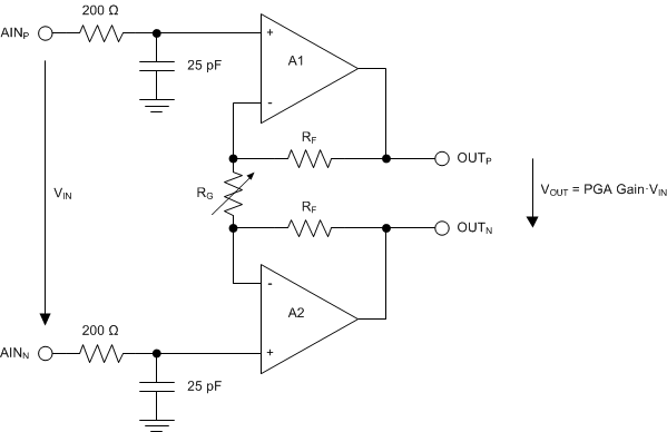
ADS122U04 pga_CMVR_bas752.gifFigure 46. Simplified PGA Diagram

VIN denotes the differential input voltage VIN = VAINP – VAINN. Use Equation 4 to calculate the gain of the PGA. Gain is changed inside the device using a variable resistor, RG.

Equation 4. PGA Gain = 1 + 2 · RF / RG

The switched-capacitor gain is changed using variable capacitors at the input to the ΔΣ modulator. Gains 1, 2, and 4 are implemented by using only the switched-capacitor circuit, which allows these gains to be used even when the PGA is bypassed; see the Bypassing the PGA section for more information about bypassing the PGA.

Equation 5 shows that the differential full-scale input voltage range (FSR) of the device is defined by the gain setting and the reference voltage used:

Equation 5. FSR = ±VREF / Gain

Table 10 shows the corresponding full-scale ranges when using the internal 2.048-V reference.

Table 10. Full-Scale Range

GAIN SETTING FSR
1 ±2.048 V
2 ±1.024 V
4 ±0.512 V
8 ±0.256 V
16 ±0.128 V
32 ±0.064 V
64 ±0.032 V
128 ±0.016 V