JAJSDR6C August 2017 – February 2022 TIC12400-Q1
PRODUCTION DATA
- 1 特長
- 2 アプリケーション
- 3 概要
- 4 Revision History
- 5 Pin Configuration and Functions
- 6 Specifications
- 7 Parameter Measurement Information
-
8 Detailed Description
- 8.1 Overview
- 8.2 Functional Block Diagram
- 8.3
Feature Description
- 8.3.1 VS Pin
- 8.3.2 VDD Pin
- 8.3.3 Device Initialization
- 8.3.4 Device Trigger
- 8.3.5 Device Reset
- 8.3.6 VS Under-Voltage (UV) Condition
- 8.3.7 VS Over-Voltage (OV) Condition
- 8.3.8 Switch Inputs Settings
- 8.3.9 Interrupt Generation and INT Assertion
- 8.3.10 Temperature Monitor
- 8.3.11 Parity Check and Parity Generation
- 8.3.12 Cyclic Redundancy Check (CRC)
- 8.4 Device Functional Modes
- 8.5 Programming
- 8.6 Register Maps
- 8.7 Programming Guidelines
- 9 Application Information Disclaimer
- 10Power Supply Recommendations
- 11Layout
- 12Device and Documentation Support
- 13Mechanical, Packaging, and Orderable Information
8.3.9.1 INT Pin Assertion Scheme
TIC12400-Q1 supports two configurable schemes for INT assertion: static and dynamic. The scheme can be adjusted by configuring the INT_CONFIG bit in the CONFIG register.
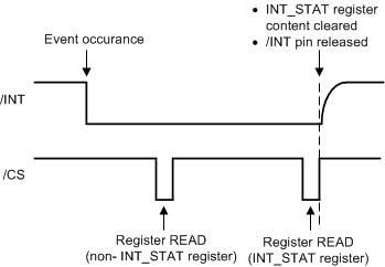
If the static INT assertion scheme is used (INT_CONFIG = 0 in the CONFIG register), the INT pin is asserted low upon occurrence of an event. The INT pin is released on the rising edge of CS only if a READ command has been issued to read the INT_STAT register while CS is low, otherwise the INT will be kept low indefinitely. The content of the INT_STAT interrupt register is latched on the first rising edge of SCLK after CS goes low for every SPI transaction, and the content is cleared upon a READ command issued to the INT_STAT register, as illustrated in Figure 8-5.
 Figure 8-5 Static
INT Assertion Scheme
Figure 8-5 Static
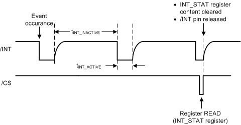
INT Assertion SchemeIn some system implementations an edge-triggered based microcontroller might potentially miss the INT assertion if it is configured to the static scheme, especially when the microcontroller is in the process of waking up. To prevent missed INT assertion and improve robustness of the interrupt behavior, the TIC12400-Q1 provides the option to use the dynamic assertion scheme for the INT pin. When the dynamic scheme is used (INT_CONFIG= 1 in the CONFIG register), the INT pin is asserted low for a duration of tINT_ACTIVE and is de-asserted back to high if the INT_STAT register has not been read after tINT_ACTIVE has elapsed. The INT is kept high for a duration of tINT_INACTIVE, and is re-asserted low after tINT_INACTIVE has elapsed. The INT pin continues to toggle until the INT_STAT register is read.
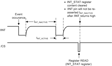
If the INT_STAT register is read when INT pin is asserted low, the INT pin is released on the READ command’s CS rising edge and the content of the INT_STAT register is also cleared, as shown in Figure 8-6. If the INT_STAT register is read when INT pin is de-asserted, the content of the INT_STAT register is cleared on the READ command’s CS rising edge, and the INT pin is not re-asserted back low, as shown in Figure 8-7.
 Figure 8-6 Dynamic
INT Assertion Scheme With INT_STAT Register Read During tINT_ACTIVE
 Figure 8-7 Dynamic
INT Assertion Scheme With INT_STAT Register Read During tINT_INACTIVE
Figure 8-7 Dynamic
INT Assertion Scheme With INT_STAT Register Read During tINT_INACTIVEThe static INT assertion scheme is selected by default upon device reset. The INT pin assertion scheme can only be changed when bit TRIGGER is logic 0 in the CONFIG register.