JAJSDR7E February 2016 – December 2019 MSP430FR2310 , MSP430FR2311
PRODUCTION DATA.
- 1デバイスの概要
- 2改訂履歴
- 3Device Comparison
- 4Terminal Configuration and Functions
-
5Specifications
- 5.1 Absolute Maximum Ratings
- 5.2 ESD Ratings
- 5.3 Recommended Operating Conditions
- 5.4 Active Mode Supply Current Into VCC Excluding External Current
- 5.5 Active Mode Supply Current Per MHz
- 5.6 Low-Power Mode LPM0 Supply Currents Into VCC Excluding External Current
- 5.7 Low-Power Mode LPM3 and LPM4 Supply Currents (Into VCC) Excluding External Current
- 5.8 Low-Power Mode LPMx.5 Supply Currents (Into VCC) Excluding External Current
- 5.9 Production Distribution of LPM Supply Currents
- 5.10 Typical Characteristics – Current Consumption Per Module
- 5.11 Thermal Resistance Characteristics
- 5.12
Timing and Switching Characteristics
- 5.12.1 Power Supply Sequencing
- 5.12.2 Reset Timing
- 5.12.3 Clock Specifications
- 5.12.4 Digital I/Os
- 5.12.5 VREF+ Built-in Reference
- 5.12.6 Timer_B
- 5.12.7
eUSCI
- Table 5-14 eUSCI (UART Mode) Clock Frequency
- Table 5-15 eUSCI (UART Mode) Switching Characteristics
- Table 5-16 eUSCI (SPI Master Mode) Clock Frequency
- Table 5-17 eUSCI (SPI Master Mode) Switching Characteristics
- Table 5-18 eUSCI (SPI Slave Mode) Switching Characteristics
- Table 5-19 eUSCI (I2C Mode) Switching Characteristics
- 5.12.8 ADC
- 5.12.9 Enhanced Comparator (eCOMP)
- 5.12.10 Smart Analog Combo (SAC)
- 5.12.11 Transimpedance Amplifier (TIA)
- 5.12.12 FRAM
- 5.12.13 Emulation and Debug
-
6Detailed Description
- 6.1 Overview
- 6.2 CPU
- 6.3 Operating Modes
- 6.4 Interrupt Vector Addresses
- 6.5 Memory Organization
- 6.6 Bootloader (BSL)
- 6.7 JTAG Standard Interface
- 6.8 Spy-Bi-Wire Interface (SBW)
- 6.9 FRAM
- 6.10 Memory Protection
- 6.11
Peripherals
- 6.11.1 Power-Management Module (PMM) and On-chip Reference Voltages
- 6.11.2 Clock System (CS) and Clock Distribution
- 6.11.3 General-Purpose Input/Output Port (I/O)
- 6.11.4 Watchdog Timer (WDT)
- 6.11.5 System Module (SYS)
- 6.11.6 Cyclic Redundancy Check (CRC)
- 6.11.7 Enhanced Universal Serial Communication Interface (eUSCI_A0, eUSCI_B0)
- 6.11.8 Timers (Timer0_B3, Timer1_B3)
- 6.11.9 Backup Memory (BAKMEM)
- 6.11.10 Real-Time Clock (RTC) Counter
- 6.11.11 10-Bit Analog-to-Digital Converter (ADC)
- 6.11.12 eCOMP0
- 6.11.13 SAC0
- 6.11.14 TIA0
- 6.11.15 eCOMP0, SAC0, TIA0, and ADC in SOC Interconnection
- 6.11.16 Embedded Emulation Module (EEM)
- 6.11.17 Peripheral File Map
- 6.12 Input/Output Diagrams
- 6.13 Device Descriptors (TLV)
- 6.14 Identification
- 7Applications, Implementation, and Layout
- 8デバイスおよびドキュメントのサポート
- 9メカニカル、パッケージ、および注文情報
Table 5-18 eUSCI (SPI Slave Mode) Switching Characteristics
over recommended ranges of supply voltage and operating free-air temperature (unless otherwise noted)(1)| PARAMETER | TEST CONDITIONS | VCC | MIN | MAX | UNIT | |
|---|---|---|---|---|---|---|
| tSTE,LEAD | STE lead time, STE active to clock | 2.0 V | 55 | ns | ||
| 3.0 V | 45 | |||||
| tSTE,LAG | STE lag time, last clock to STE inactive | 2.0 V | 20 | ns | ||
| 3.0 V | 20 | |||||
| tSTE,ACC | STE access time, STE active to SOMI data out | 2.0 V | 65 | ns | ||
| 3.0 V | 40 | |||||
| tSTE,DIS | STE disable time, STE inactive to SOMI high impedance | 2.0 V | 40 | ns | ||
| 3.0 V | 35 | |||||
| tSU,SI | SIMO input data setup time | 2.0 V | 8 | ns | ||
| 3.0 V | 6 | |||||
| tHD,SI | SIMO input data hold time | 2.0 V | 12 | ns | ||
| 3.0 V | 12 | |||||
| tVALID,SO | SOMI output data valid time(2) | UCLK edge to SOMI valid,
CL = 20 pF |
2.0 V | 68 | ns | |
| 3.0 V | 42 | |||||
| tHD,SO | SOMI output data hold time (3) | CL = 20 pF | 2.0 V | 5 | ns | |
| 3.0 V | 5 | |||||
(1) fUCxCLK = 1/2tLO/HI with tLO/HI ≥ max(tVALID,MO(Master) + tSU,SI(eUSCI), tSU,MI(Master) + tVALID,SO(eUSCI))
For the master parameters tSU,MI(Master) and tVALID,MO(Master), see the SPI parameters of the attached master.
For the master parameters tSU,MI(Master) and tVALID,MO(Master), see the SPI parameters of the attached master.
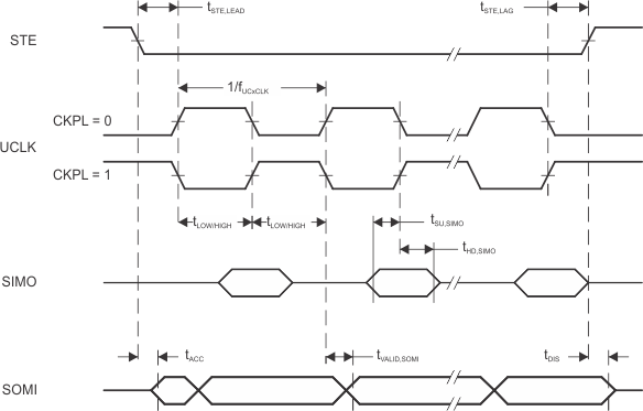
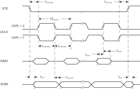
(2) Specifies the time to drive the next valid data to the SOMI output after the output changing UCLK clock edge. See the timing diagrams in Figure 5-12 and Figure 5-13.
(3) Specifies how long data on the SOMI output is valid after the output changing UCLK clock edge. See the timing diagrams in Figure 5-12 and Figure 5-13.
 Figure 5-12 SPI Slave Mode, CKPH = 0
  Figure 5-13 SPI Slave Mode, CKPH = 1
 Table 5-19 lists the switching characteristics of the eUSCI (I2C mode).