JAJSDX8E June 2017 – August 2018 ISO1211 , ISO1212
PRODUCTION DATA.
- 1 特長
- 2 アプリケーション
- 3 概要
- 4 改訂履歴
- 5 概要(続き)
- 6 Pin Configuration and Functions
-
7 Specifications
- 7.1 Absolute Maximum Ratings
- 7.2 ESD Ratings
- 7.3 Recommended Operating Conditions
- 7.4 Thermal Information
- 7.5 Power Ratings
- 7.6 Insulation Specifications
- 7.7 Safety-Related Certifications
- 7.8 Safety Limiting Values
- 7.9 Electrical Characteristics—DC Specification
- 7.10 Switching Characteristics—AC Specification
- 7.11 Insulation Characteristics Curves
- 7.12 Typical Characteristics
- 8 Parameter Measurement Information
- 9 Detailed Description
-
10Application and Implementation
- 10.1 Application Information
- 10.2
Typical Application
- 10.2.1
Sinking Inputs
- 10.2.1.1 Design Requirements
- 10.2.1.2
Detailed Design Procedure
- 10.2.1.2.1 Setting Current Limit and Voltage Thresholds
- 10.2.1.2.2 Thermal Considerations
- 10.2.1.2.3 Designing for 48-V Systems
- 10.2.1.2.4 Designing for Input Voltages Greater Than 60 V
- 10.2.1.2.5 Surge, ESD, and EFT Tests
- 10.2.1.2.6 Multiplexing the Interface to the Host Controller
- 10.2.1.2.7 Status LEDs
- 10.2.1.3 Application Curve
- 10.2.2 Sourcing Inputs
- 10.2.3 Sourcing and Sinking Inputs (Bidirectional Inputs)
- 10.2.1
Sinking Inputs
- 11Power Supply Recommendations
- 12Layout
- 13デバイスおよびドキュメントのサポート
- 14メカニカル、パッケージ、および注文情報
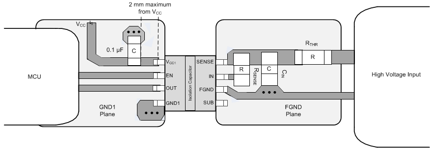
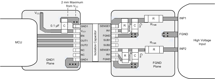
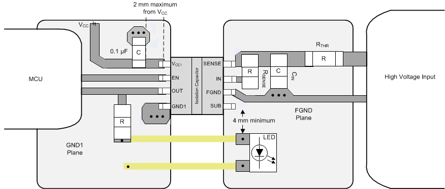
12.2 Layout Example
 Figure 31. Layout Example With ISO1211
  Figure 32. Layout Example With ISO1212
  Figure 33. Layout Example With LED Placed on the Field Side But Driven From VCC1 Power Domain