JAJSDY0F July   2017  – December 2021 TPS22916

PRODUCTION DATA  

  1. 特長
  2. アプリケーション
  3. 概要
  4. Revision History
  5. Pin Configuration and Functions
  6. Specifications
    1. 6.1 Absolute Maximum Ratings
    2. 6.2 ESD Ratings
    3. 6.3 Recommended Operating Conditions
    4. 6.4 Thermal Information
    5. 6.5 Electrical Characteristics
    6. 6.6 Switching Characteristics
    7. 6.7 Typical Characteristics
      1. 6.7.1 Typical Electrical Characteristics
      2. 6.7.2 Typical Switching Characteristics
  7. Parameter Measurement Information
  8. Detailed Description
    1. 8.1 Overview
    2. 8.2 Functional Block Diagram
    3. 8.3 Feature Description
      1. 8.3.1 On and Off Control
      2. 8.3.2 Fall Time (tFALL) and Quick Output Discharge (QOD)
      3. 8.3.3 Full-Time Reverse Current Blocking
    4. 8.4 Device Functional Modes
  9. Application and Implementation
    1. 9.1 Application Information
    2. 9.2 Typical Application
      1. 9.2.1 Design Requirements
      2. 9.2.2 Detailed Design Procedure
        1. 9.2.2.1 Maximum Inrush Current
      3. 9.2.3 Application Curve
  10. 10Power Supply Recommendations
  11. 11Layout
    1. 11.1 Layout Guidelines
    2. 11.2 Layout Example
    3. 11.3 Thermal Considerations
  12. 12Device and Documentation Support
    1. 12.1 Documentation Support
      1. 12.1.1 Related Documentation
    2. 12.2 Receiving Notification of Documentation Updates
    3. 12.3 サポート・リソース
    4. 12.4 Trademarks
    5. 12.5 Electrostatic Discharge Caution
    6. 12.6 Glossary
  13. 13Mechanical, Packaging, and Orderable Information
    1. 13.1 Tape and Reel Information

Layout Example

Equation 3 shows an example for these devices. Notice the connection to system ground between the VOUT Bypass Capacitor ground and the GND pin of the load switch,. This connection creates a ground barrier which helps to reduce the ground noise seen by the device.
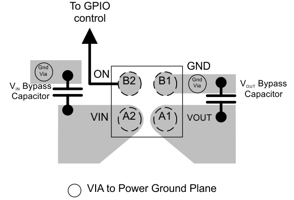
GUID-DD682C4C-AD1F-4D2E-8421-488162D115C4-low.gifFigure 11-1 TPS22916xx Layout