JAJSE18E March 2017 – May 2021 CC3220MOD , CC3220MODA
PRODUCTION DATA
- 1 特長
- 2 アプリケーション
- 3 概要
- 4 機能ブロック図
- 5 Revision History
- 6 Device Comparison
- 7 Terminal Configuration and Functions
-
8 Specifications
- 8.1 Absolute Maximum Ratings
- 8.2 ESD Ratings
- 8.3 Recommended Operating Conditions
- 8.4 Current Consumption (CC3220MODS and CC3220MODAS)
- 8.5 Current Consumption (CC3220MODSF and CC3220MODASF)
- 8.6 TX Power and IBAT Versus TX Power Level Settings
- 8.7 Brownout and Blackout Conditions
- 8.8 Electrical Characteristics
- 8.9 CC3220MODAx Antenna Characteristics
- 8.10 WLAN Receiver Characteristics
- 8.11 WLAN Transmitter Characteristics
- 8.12 Reset Requirement
- 8.13 Thermal Resistance Characteristics for MOB and MON Packages
- 8.14
Timing and Switching Characteristics
- 8.14.1 Power-Up Sequencing
- 8.14.2 Power-Down Sequencing
- 8.14.3 Device Reset
- 8.14.4 Wake Up From Hibernate Timing
- 8.14.5 Peripherals Timing
-
9 Detailed Description
- 9.1 Overview
- 9.2 Arm® Cortex®-M4 プロセッサ・コア・サブシステム
- 9.3 Wi-Fi® Network Processor Subsystem
- 9.4 Security
- 9.5 Power-Management Subsystem
- 9.6 Low-Power Operating Mode
- 9.7 Memory
- 9.8 Restoring Factory Default Configuration
- 9.9 Boot Modes
- 9.10 Device Certification and Qualification
- 9.11 Module Markings
- 9.12 End Product Labeling
- 9.13 Manual Information to the End User
- 10Applications, Implementation, and Layout
- 11Environmental Requirements and Specifications
- 12Device and Documentation Support
- 13Mechanical, Packaging, and Orderable Information
8.14.5.5 IEEE 1149.1 JTAG
The Joint Test Action Group (JTAG) port is an IEEE standard that defines a test access port (TAP) and boundary scan architecture for digital integrated circuits and provides a standardized serial interface to control the associated test logic. For detailed information on the operation of the JTAG port and TAP controller, see the IEEE Standard 1149.1,Test Access Port and Boundary-Scan Architecture.
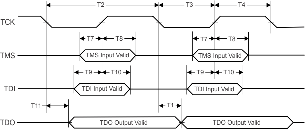
Figure 8-14 shows the JTAG timing diagram.
 Figure 8-14 JTAG
Timing Diagram
Table 8-12 lists the JTAG timing parameters.
Table 8-12 JTAG Timing Parameters
| ITEM | NAME | DESCRIPTION | MIN | MAX | UNIT |
|---|---|---|---|---|---|
| T1 | fTCK | Clock frequency | 15 | MHz | |
| T2 | tTCK | Clock period | 1 / fTCK | ns | |
| T3 | tCL | Clock low period | tTCK / 2 | ns | |
| T4 | tCH | Clock high period | tTCK / 2 | ns | |
| T7 | tTMS_SU | TMS setup time | 1 | ns | |
| T8 | tTMS_HO | TMS hold time | 16 | ns | |
| T9 | tTDI_SU | TDI setup time | 1 | ns | |
| T10 | tTDI_HO | TDI hold time | 16 | ns | |
| T11 | tTDO_HO | TDO hold time | 15 | ns |