JAJSE19G October   2017  – November 2022 TUSB564

PRODUCTION DATA  

  1. 特長
  2. アプリケーション
  3. 概要
  4. Revision History
  5. Pin Configuration and Functions
  6. Specifications
    1. 6.1 Absolute Maximum Ratings
    2. 6.2 ESD Ratings
    3. 6.3 Recommended Operating Conditions
    4. 6.4 Thermal Information
    5. 6.5 Electrical Characteristics
    6. 6.6 Switching Characteristics
    7. 6.7 Timing Requirements
    8. 6.8 Typical Characteristics
  7. Parameter Measurement Information
  8. Detailed Description
    1. 8.1 Overview
    2. 8.2 Functional Block Diagram
    3. 8.3 Feature Description
      1. 8.3.1 USB 3.1
      2. 8.3.2 DisplayPort
      3. 8.3.3 4-Level Inputs
      4. 8.3.4 Receiver Linear Equalization
    4. 8.4 Device Functional Modes
      1. 8.4.1 Device Configuration in GPIO Mode
      2. 8.4.2 Device Configuration In I2C Mode
      3. 8.4.3 DisplayPort Mode
      4. 8.4.4 Linear EQ Configuration
      5. 8.4.5 USB3.1 Modes
      6. 8.4.6 Operation Timing – Power Up
    5. 8.5 Programming
    6. 8.6 Register Maps
      1. 8.6.1 General Register (address = 0x0A) [reset = 00000001]
      2. 8.6.2 DisplayPort Control/Status Registers (address = 0x10) [reset = 00000000]
      3. 8.6.3 DisplayPort Control/Status Registers (address = 0x11) [reset = 00000000]
      4. 8.6.4 DisplayPort Control/Status Registers (address = 0x12) [reset = 00000000]
      5. 8.6.5 DisplayPort Control/Status Registers (address = 0x13) [reset = 00000000]
      6. 8.6.6 USB3.1 Control/Status Registers (address = 0x20) [reset = 00000000]
      7. 8.6.7 USB3.1 Control/Status Registers (address = 0x21) [reset = 00000000]
      8. 8.6.8 USB3.1 Control/Status Registers (address = 0x22) [reset = 00000000]
  9. Application and Implementation
    1. 9.1 Application Information
    2. 9.2 Typical Application
      1. 9.2.1 Design Requirements
      2. 9.2.2 Detailed Design Procedure
      3. 9.2.3 Support for DisplayPort UFP_D Pin Assignment E
      4. 9.2.4 PCB Insertion Loss Curves
    3. 9.3 System Examples
      1. 9.3.1 USB 3.1 Only
      2. 9.3.2 USB 3.1 and 2 Lanes of DisplayPort
      3. 9.3.3 DisplayPort Only
  10. 10Power Supply Recommendations
  11. 11Layout
    1. 11.1 Layout Guidelines
    2. 11.2 Layout Example
  12. 12Device and Documentation Support
    1. 12.1 Receiving Notification of Documentation Updates
    2. 12.2 サポート・リソース
    3. 12.3 Trademarks
    4. 12.4 Electrostatic Discharge Caution
    5. 12.5 Glossary
  13. 13Mechanical, Packaging, and Orderable Information

Typical Characteristics

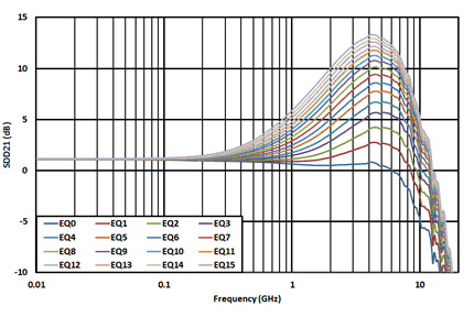
GUID-E7F4D438-B652-4A6D-B2B8-984FF92ABB06-low.gif
Figure 6-1 DisplayPort EQ Settings Curves
GUID-0ADA4CA2-547F-43C7-AEAF-3267DEF1FB46-low.gif
Figure 6-3 USB TX (UFP) EQ Settings Curves
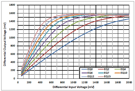
GUID-7E19CB48-A89A-4F8C-8990-7377F04FC44F-low.gif
Figure 6-5 USB TX (DFP) Linearity Curves at 2.5 GHz
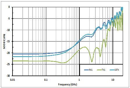
GUID-BDAE7494-BEE3-45CB-98BD-694446A82749-low.gif
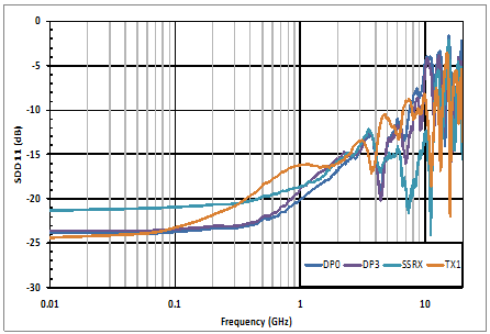
Figure 6-7 Input Return Loss Performance
GUID-F947EFF8-481D-40F2-AC31-A62A6C930169-low.gif
Figure 6-9 DisplayPort HBR3 Eye-Pattern Performance with 12-inch Input PCB Trace at 8.1 Gbps
GUID-09BC2794-CC43-422F-B30E-A06429616C82-low.gif
Figure 6-2 USB RX (DFP) EQ Settings Curves
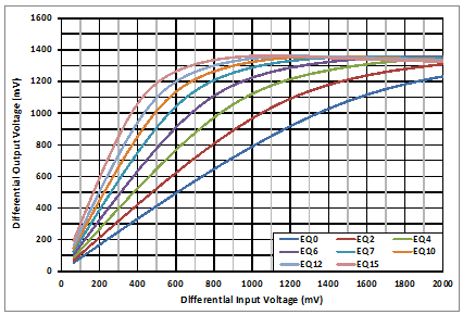
GUID-B1909A38-2378-4E28-97A7-8AF710B28FB7-low.gif
Figure 6-4 DisplayPort Linearity Curves at 4.05 GHz
GUID-96122EE6-0922-4993-BD45-6333BAD63E4D-low.gif
Figure 6-6 USB RX (UFP) Linearity Curves at 2.5 GHz
GUID-FB51A5CE-936E-4B16-8F3A-E1BDA94D8424-low.gif
Figure 6-8 Output Return Loss Performance
GUID-D05AD27D-FAE6-4272-B1B1-352653562886-low.gif
Figure 6-10 USB 3.1 Gen1 Eye-Pattern Performance with 12-inch Input PCB Trace at 5 Gbps