JAJSE19G October 2017 – November 2022 TUSB564
PRODUCTION DATA
- 1 特長
- 2 アプリケーション
- 3 概要
- 4 Revision History
- 5 Pin Configuration and Functions
- 6 Specifications
- 7 Parameter Measurement Information
-
8 Detailed Description
- 8.1 Overview
- 8.2 Functional Block Diagram
- 8.3 Feature Description
- 8.4 Device Functional Modes
- 8.5 Programming
- 8.6
Register Maps
- 8.6.1 General Register (address = 0x0A) [reset = 00000001]
- 8.6.2 DisplayPort Control/Status Registers (address = 0x10) [reset = 00000000]
- 8.6.3 DisplayPort Control/Status Registers (address = 0x11) [reset = 00000000]
- 8.6.4 DisplayPort Control/Status Registers (address = 0x12) [reset = 00000000]
- 8.6.5 DisplayPort Control/Status Registers (address = 0x13) [reset = 00000000]
- 8.6.6 USB3.1 Control/Status Registers (address = 0x20) [reset = 00000000]
- 8.6.7 USB3.1 Control/Status Registers (address = 0x21) [reset = 00000000]
- 8.6.8 USB3.1 Control/Status Registers (address = 0x22) [reset = 00000000]
- 9 Application and Implementation
- 10Power Supply Recommendations
- 11Layout
- 12Device and Documentation Support
- 13Mechanical, Packaging, and Orderable Information
9.2.3 Support for DisplayPort UFP_D Pin Assignment E
The TUSB564 device can be used in a system that handles DisplayPort UFP_D Pin Assignment E use-case if special measures are taken as described below. With UFP_D Pin Assignment E, the polarity of both the main link and AUX signals is inverted on the Type-C receptacle pins relative to Pin Assignment C. Moreover, on the Type-C receptacle, the location of Lane 0 is swapped with Lane 1 and that of Lane 2 is swapped with Lane 3 relative to Pin Assignment C. For correct reception of the DisplayPort video signal, the system has to comprehend the above-described signaling variation.
The use of the TUSB564 device in a system that handles Pin Assignment E depends on whether AUX-to-SBU switching of the DisplayPort AUX signal is performed internally by the TUSB564 or by external devices such as a PD controller. It also depends on the configuration mode used: I2C Mode or GPIO Mode. In all those scenarios the TUSB564 passes the polarity of the Main Link signals as received. The DisplayPort sink has to handle the polarity inversion of those signals. Moreover, the DisplayPort sink has to handle the lane swapping with the following lane-to-pin mapping as received by the TUSB564 device: Lane 0 → DP1, Lane 1 → DP0, Lane 2 → DP3, and Lane 3 → DP2.
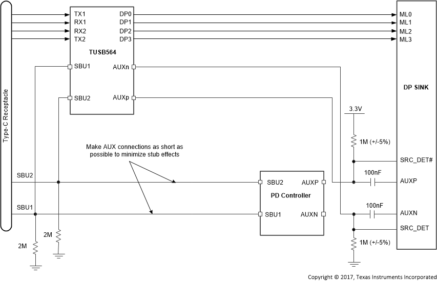
The use-case with the AUX-to-SBU switching performed internally by the TUSB564 device is shown in Figure 9-3. If the TUSB564 device configuration is through the I2C Mode, AUX snooping has to be disabled by setting AUX_SNOOP_DISABLE register 0x13[7] = 1'b1, and manual AUX-to-SBU switching has to be performed through the AUX_SBU_OVR register 0x13[5:4]: AUX_SBU_OVR = 2’b01 for normal USB Type-C plug orientation, or AUX_SBU_OVR = 2’b10 for flipped USB Type-C plug orientation when Pin Assignment E signals are received. If the TUSB564 device configuration is through the GPIO Mode, all 4 DisplayPort lanes are automatically activated. The DisplayPort sink device has to handle the polarity inversion of both the AUX and Main Link signals as well as main link lane swapping.
 Figure 9-3 DisplayPort AUX Connections
for UFP_D Pin Assignment E with Internal AUX Switching
Figure 9-3 DisplayPort AUX Connections
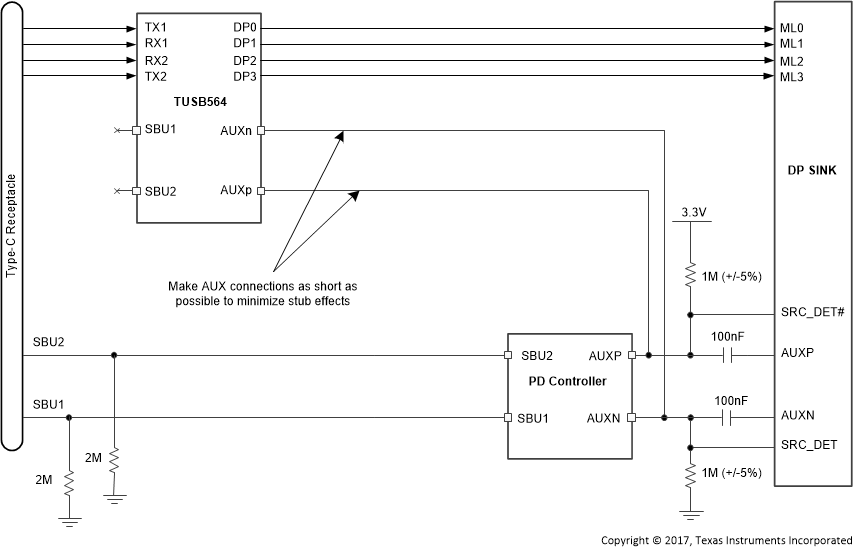
for UFP_D Pin Assignment E with Internal AUX SwitchingThe use-case with the AUX-to-SBU switching performed by an external device is shown in Figure 9-4. In this case, it is assumed that the PD controller is capable of correcting the polarity inversion of the AUX signal and the TUSB564 is provided with the corrected polarity of the AUX signal through its AUXp/AUXn pins. If the TUSB564 device configuration is through the I2C Mode, AUX snooping should be disabled by setting AUX_SNOOP_DISABLE register 0x13[7] = 1'b1. The DisplayPort sink device has to handle the polarity inversion of the Main Link signals as well as the Main Link lane swapping.
 Figure 9-4 DisplayPort AUX Connections
for UFP_D Pin Assignment E with External AUX Switching