JAJSE19G October 2017 – November 2022 TUSB564
PRODUCTION DATA
- 1 特長
- 2 アプリケーション
- 3 概要
- 4 Revision History
- 5 Pin Configuration and Functions
- 6 Specifications
- 7 Parameter Measurement Information
-
8 Detailed Description
- 8.1 Overview
- 8.2 Functional Block Diagram
- 8.3 Feature Description
- 8.4 Device Functional Modes
- 8.5 Programming
- 8.6
Register Maps
- 8.6.1 General Register (address = 0x0A) [reset = 00000001]
- 8.6.2 DisplayPort Control/Status Registers (address = 0x10) [reset = 00000000]
- 8.6.3 DisplayPort Control/Status Registers (address = 0x11) [reset = 00000000]
- 8.6.4 DisplayPort Control/Status Registers (address = 0x12) [reset = 00000000]
- 8.6.5 DisplayPort Control/Status Registers (address = 0x13) [reset = 00000000]
- 8.6.6 USB3.1 Control/Status Registers (address = 0x20) [reset = 00000000]
- 8.6.7 USB3.1 Control/Status Registers (address = 0x21) [reset = 00000000]
- 8.6.8 USB3.1 Control/Status Registers (address = 0x22) [reset = 00000000]
- 9 Application and Implementation
- 10Power Supply Recommendations
- 11Layout
- 12Device and Documentation Support
- 13Mechanical, Packaging, and Orderable Information
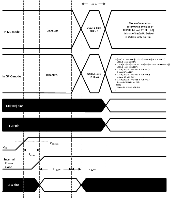
8.4.6 Operation Timing – Power Up
 Figure 8-1 Power-Up Timing
Table 8-8 Power-Up Timing(1)(2)
| PARAMETER | MIN | MAX | UNIT | |
|---|---|---|---|---|
| td_pg | VCC (minimum) to Internal Power Good asserted high | 500 | µs | |
| tcfg_su | CFG(1) pins setup(2) | 50 | µs | |
| tcfg_hd | CFG(1) pins hold | 10 | µs | |
| tCTL_DB | CTL[1:0] and FLIP pin debounce | 16 | ms | |
| tVCC_RAMP | VCC supply ramp requirement | 0.1 | 100 | ms |
(1) Following pins comprise CFG pins: I2C_EN, EQ[1:0], SSEQ[1:0], and DPEQ[1:0].
(2) Recommend CFG pins are stable when VCC is at minimum value.