JAJSE44B May 2017 – April 2018 IWR1642
PRODUCTION DATA.
- 1 デバイスの概要
- 2 改訂履歴
- 3 Device Comparison
- 4 Terminal Configuration and Functions
-
5 Specifications
- 5.1 Absolute Maximum Ratings
- 5.2 ESD Ratings
- 5.3 Power-On Hours (POH)
- 5.4 Recommended Operating Conditions
- 5.5 Power Supply Specifications
- 5.6 Power Consumption Summary
- 5.7 RF Specification
- 5.8 CPU Specifications
- 5.9 Thermal Resistance Characteristics for FCBGA Package [ABL0161]
- 5.10
Timing and Switching Characteristics
- 5.10.1 Power Supply Sequencing and Reset Timing
- 5.10.2 Input Clocks and Oscillators
- 5.10.3
Multibuffered / Standard Serial Peripheral Interface (MibSPI)
- 5.10.3.1 Peripheral Description
- 5.10.3.2
MibSPI Transmit and Receive RAM Organization
- Table 5-7 SPI Timing Conditions
- Table 5-8 SPI Master Mode Switching Parameters (CLOCK PHASE = 0, SPICLK = output, SPISIMO = output, and SPISOMI = input)
- Table 5-9 SPI Master Mode Input Timing Requirements (CLOCK PHASE = 0, SPICLK = output, SPISIMO = output, and SPISOMI = input)
- Table 5-10 SPI Master Mode Switching Parameters (CLOCK PHASE = 1, SPICLK = output, SPISIMO = output, and SPISOMI = input)
- Table 5-11 SPI Master Mode Input Requirements (CLOCK PHASE = 1, SPICLK = output, SPISIMO = output, and SPISOMI = input)
- 5.10.3.3 SPI Slave Mode I/O Timings
- 5.10.3.4 Typical Interface Protocol Diagram (Slave Mode)
- 5.10.4 LVDS Interface Configuration
- 5.10.5 General-Purpose Input/Output
- 5.10.6 Controller Area Network Interface (DCAN)
- 5.10.7 Serial Communication Interface (SCI)
- 5.10.8 Inter-Integrated Circuit Interface (I2C)
- 5.10.9 Quad Serial Peripheral Interface (QSPI)
- 5.10.10 ETM Trace Interface
- 5.10.11 Data Modification Module (DMM)
- 5.10.12 JTAG Interface
- 6 Detailed Description
- 7 Monitoring and Diagnostics
- 8 Applications, Implementation, and Layout
- 9 Device and Documentation Support
- 10Mechanical, Packaging, and Orderable Information
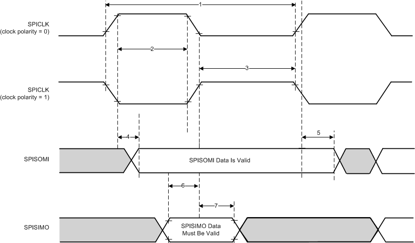
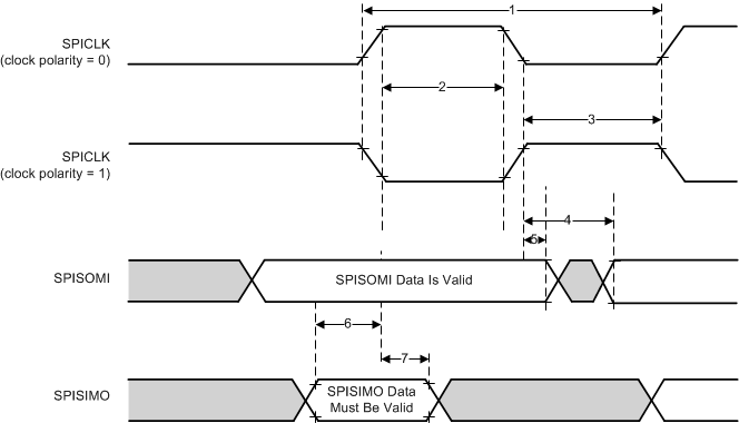
Table 5-13 SPI Slave Mode Timing Requirements (SPICLK = input, SPISIMO = input,
and SPISOMI = output)
| NO. | MIN | TYP | MAX | UNIT | |||
|---|---|---|---|---|---|---|---|
| 6(1) | tsu(SIMO-SPCL)S | Setup time, SPISIMO before SPICLK low (clock polarity = 0) | 3 | ns | |||
| tsu(SIMO-SPCH)S | Setup time, SPISIMO before SPICLK high (clock polarity = 1) | 3 | |||||
| 7(1) | th(SPCL-SIMO)S | Hold time, SPISIMO data valid after SPICLK low (clock polarity = 0) | 0 | ns | |||
| th(SPCL-SIMO)S | Hold time, SPISIMO data valid after SPICLK low (clock polarity = 0) | 0 | |||||
| 6(1) | tsu(SIMO-SPCL)S | Setup time, SPISIMO before SPICLK low (clock polarity = 0; clock phase = 0) OR (clock polarity = 1; clock phase = 1) | 3 | ns | |||
| tsu(SIMO-SPCH)S | Setup time, SPISIMO before SPICLK high (clock polarity = 1; clock phase = 0) OR (clock polarity = 0; clock phase = 1) | 3 | |||||
| 7(1) | th(SPCL-SIMO)S | Hold time, SPISIMO data valid after SPICLK low (clock polarity = 0; clock phase = 0) OR (clock polarity = 1; clock phase = 1) | 1 | ns | |||
| th(SPCL-SIMO)S | Hold time, SPISIMO data valid after SPICLK high (clock polarity = 1; clock phase = 0) OR (clock polarity = 0; clock phase = 1) | 1 | |||||
(1) The active edge of the SPICLK signal referenced is controlled by the CLOCK POLARITY bit (SPIFMTx.17).
 Figure 5-8 SPI Slave Mode External Timing (CLOCK PHASE = 0)
  Figure 5-9 SPI Slave Mode External Timing (CLOCK PHASE = 1)