JAJSE57E March 2013 – October 2017 LMT85
PRODUCTION DATA.
7 Specifications
7.1 Absolute Maximum Ratings
See (1)(3)| MIN | MAX | UNIT | ||
|---|---|---|---|---|
| Supply voltage | −0.3 | 6 | V | |
| Voltage at output pin | −0.3 | (VDD + 0.5) | V | |
| Output current | –7 | 7 | mA | |
| Input current at any pin (2) | –5 | 5 | mA | |
| Maximum junction temperature (TJMAX) | 150 | °C | ||
| Storage temperature, Tstg | –65 | 150 | °C | |
(1) Stresses beyond those listed under Absolute Maximum Ratings may cause permanent damage to the device. These are stress ratings only, which do not imply functional operation of the device at these or any other conditions beyond those indicated under Recommended Operating Conditions. Exposure to absolute-maximum-rated conditions for extended periods may affect device reliability
(2) When the input voltage (VI) at any pin exceeds power supplies (VI < GND or VI > V), the current at that pin should be limited to 5 mA.
(3) Soldering process must comply with Reflow Temperature Profile specifications. Refer towww.ti.com/packaging .
7.2 ESD Ratings
| VALUE | UNIT | |||
|---|---|---|---|---|
| LMT85LP in TO-92/TO-92S package | ||||
| V(ESD) | Electrostatic discharge | Human-body model (HBM), per ANSI/ESDA/JEDEC JS-001(1)(3) | ±2500 | V |
| Charged-device model (CDM), per JEDEC specification JESD22-C101(2) | ±1000 | |||
| LMT85DCK in SC70 package | ||||
| V(ESD) | Electrostatic discharge | Human-body model (HBM), per JESD22-A114(3) | ±2500 | V |
| Charged-device model (CDM), per JEDEC specification JESD22-C101(2) | ±1000 | |||
(1) JEDEC document JEP155 states that 500-V HBM allows safe manufacturing with a standard ESD control process.
(2) JEDEC document JEP157 states that 250-V CDM allows safe manufacturing with a standard ESD control process.
(3) The human body model is a 100-pF capacitor discharged through a 1.5-kΩ resistor into each pin.
7.3 Recommended Operating Conditions
| MIN | MAX | UNIT | |
|---|---|---|---|
| Specified temperature | TMIN ≤ TA ≤ TMAX | °C | |
| −50 ≤ TA ≤ 150 | °C | ||
| Supply voltage (VDD) | 1.8 | 5.5 | V |
7.4 Thermal Information(1)
| THERMAL METRIC(2) | LMT85/ LMT85-Q1 |
LMT85LP | LMT85LPG | UNIT | |
|---|---|---|---|---|---|
| DCK (SOT/SC70) | LP/LPM (TO-92) | LPG (TO-92S) | |||
| 5 PINS | 3 PINS | 3 PINS | |||
| RθJA | Junction-to-ambient thermal resistance (3)(4) | 275 | 167 | 130.4 | °C/W |
| RθJC(top) | Junction-to-case (top) thermal resistance | 84 | 90 | 64.2 | °C/W |
| RθJB | Junction-to-board thermal resistance | 56 | 146 | 106.2 | °C/W |
| ψJT | Junction-to-top characterization parameter | 1.2 | 35 | 14.6 | °C/W |
| ψJB | Junction-to-board characterization parameter | 55 | 146 | 106.2 | °C/W |
(1) For information on self-heating and thermal response time, see section Mounting and Thermal Conductivity.
(2) For more information about traditional and new thermal metrics, see the IC Package Thermal Metrics application report.
(3) The junction to ambient thermal resistance (RθJA) under natural convection is obtained in a simulation on a JEDEC-standard, High-K board as specified in JESD51-7, in an environment described in JESD51-2. Exposed pad packages assume that thermal vias are included in the PCB, per JESD 51-5.
(4) Changes in output due to self-heating can be computed by multiplying the internal dissipation by the thermal resistance.
7.5 Accuracy Characteristics
These limits do not include DC load regulation. These stated accuracy limits are with reference to the values in Table 3.| PARAMETER | TEST CONDITIONS | MIN(1) | TYP(2) | MAX(1) | UNIT |
|---|---|---|---|---|---|
| Temperature accuracy (3) | TA = TJ= 20°C to 150°C; VDD = 1.8 V to 5.5 V | –2.7 | ±0.4 | 2.7 | °C |
| TA = TJ= 0°C to 150°C; VDD = 1.9 V to 5.5 V | –2.7 | ±0.7 | 2.7 | °C | |
| TA = TJ= 0°C to 150°C; VDD = 2.6 V to 5.5 V | ±0.3 | °C | |||
| TA = TJ= –50°C to 0°C; VDD = 2.3 V to 5.5 V | –2.7 | ±0.7 | 2.7 | °C | |
| TA = TJ= –50°C to 0°C; VDD = 2.9 V to 5.5 V | ±0.25 | °C |
(1) Limits are specific to TI's AOQL (Average Outgoing Quality Level).
(2) Typicals are at TJ = TA = 25°C and represent most likely parametric norm.
(3) Accuracy is defined as the error between the measured and reference output voltages, tabulated in the Transfer Table at the specified conditions of supply gain setting, voltage, and temperature (expressed in °C). Accuracy limits include line regulation within the specified conditions. Accuracy limits do not include load regulation; they assume no DC load.
7.6 Electrical Characteristics
Unless otherwise noted, these specifications apply for VDD = +1.8V to +5.5V. MIN and MAX limits apply for TA = TJ = TMIN to TMAX, unless otherwise noted; typical values apply for TA = TJ = 25°C.| PARAMETER | TEST CONDITIONS | MIN (1) | TYP (2) | MAX (1) | UNIT | ||
|---|---|---|---|---|---|---|---|
| Average sensor gain (output transfer function slope) | –30°C and 90°C used to calculate average sensor gain | –8.2 | mV/°C | ||||
| Load regulation (3) | Source ≤ 50 μA, (VDD - VOUT) ≥ 200 mV | –1 | –0.22 | mV | |||
| Sink ≤ 50 μA, VOUT ≥ 200 mV | 0.26 | 1 | mV | ||||
| Line regulation (4) | 200 | μV/V | |||||
| IS | Supply current | TA = TJ = 30°C to 150°C, (VDD - VOUT) ≥ 100 mV | 5.4 | 8.1 | μA | ||
| TA = TJ = -50°C to 150°C, (VDD - VOUT) ≥ 100 mV | 5.4 | 9 | μA | ||||
| CL | Output load capacitance | 1100 | pF | ||||
| Power-on time (5) | CL= 0 pF to 1100 pF | 0.7 | 1.9 | ms | |||
| Output drive | TA = TJ = 25°C | –50 | +50 | µA | |||
(1) Limits are specific to TI's AOQL (Average Outgoing Quality Level).
(2) Typicals are at TJ = TA = 25°C and represent most likely parametric norm.
(3) Source currents are flowing out of the LMT85. Sink currents are flowing into the LMT85.
(4) Line regulation (DC) is calculated by subtracting the output voltage at the highest supply voltage from the output voltage at the lowest supply voltage. The typical DC line regulation specification does not include the output voltage shift discussed in Output Voltage Shift.
(5) Specified by design and characterization.
7.7 Typical Characteristics
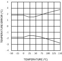 Figure 1. Temperature Error vs Temperature
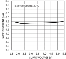
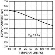 Figure 3. Supply Current vs Temperature
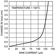
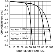 Figure 5. Load Regulation, Sourcing Current
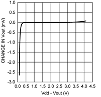 Figure 7. Change in Vout vs Overhead Voltage
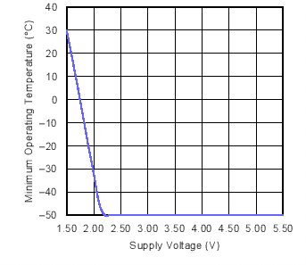
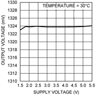 Figure 9. Output Voltage vs Supply Voltage
