JAJSE58E January   2014  – October 2017 LMT87

PRODUCTION DATA.  

  1. 特長
  2. アプリケーション
  3. 概要
    1.     Device Images
      1.      熱時定数
      2.      出力電圧と温度との関係
  4. 改訂履歴
  5. Device Comparison Tables
  6. Pin Configuration and Functions
    1.     Pin Functions
  7. Specifications
    1. 7.1 Absolute Maximum Ratings
    2. 7.2 ESD Ratings
    3. 7.3 Recommended Operating Conditions
    4. 7.4 Thermal Information
    5. 7.5 Accuracy Characteristics
    6. 7.6 Electrical Characteristics
    7. 7.7 Typical Characteristics
  8. Detailed Description
    1. 8.1 Overview
    2. 8.2 Functional Block Diagram
    3. 8.3 Feature Description
      1. 8.3.1 LMT87 Transfer Function
    4. 8.4 Device Functional Modes
      1. 8.4.1 Mounting and Thermal Conductivity
      2. 8.4.2 Output Noise Considerations
      3. 8.4.3 Capacitive Loads
      4. 8.4.4 Output Voltage Shift
  9. Application and Implementation
    1. 9.1 Application Information
    2. 9.2 Typical Applications
      1. 9.2.1 Connection to ADC
        1. 9.2.1.1 Design Requirements
        2. 9.2.1.2 Detailed Design Procedure
        3. 9.2.1.3 Application Curve
      2. 9.2.2 Conserving Power Dissipation With Shutdown
        1. 9.2.2.1 Design Requirements
        2. 9.2.2.2 Detailed Design Procedure
        3. 9.2.2.3 Application Curves
  10. 10Power Supply Recommendations
  11. 11Layout
    1. 11.1 Layout Guidelines
    2. 11.2 Layout Example
  12. 12デバイスおよびドキュメントのサポート
    1. 12.1 ドキュメントの更新通知を受け取る方法
    2. 12.2 コミュニティ・リソース
    3. 12.3 商標
    4. 12.4 静電気放電に関する注意事項
    5. 12.5 Glossary
  13. 13メカニカル、パッケージ、および注文情報

Application Curves

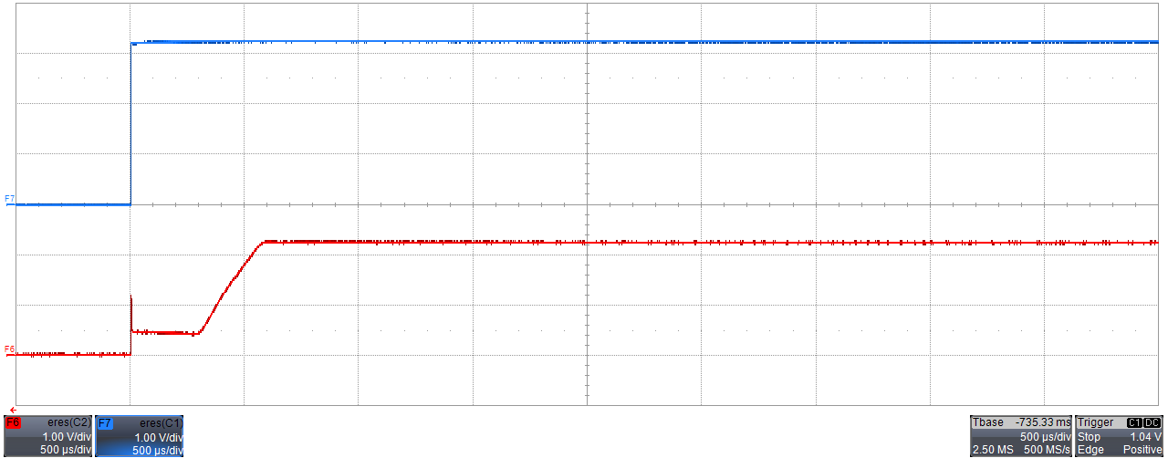
LMT87 LMT87_SNIS170_3p3_nl_resptim.png

INDENT:

Time: 500 μs/div; Top trace: VDD 1 V/div;
Bottom trace: OUT 1 V/div
Figure 16. Output Turnon Response Time Without a Capacitive Load and VDD = 3.3 V
LMT87 LMT87_SNIS170_5p0_nl_resptim.png

INDENT:

Time: 500 μs/div; Top trace: VDD 2 V/div;
Bottom trace: OUT 1 V/div
Figure 18. Output Turnon Response Time Without a Capacitive Load and VDD = 5 V
LMT87 LMT87_SNIS170_3p3_1NF_resptim.png

INDENT:

Time: 500 μs/div; Top trace: VDD 1 V/div;
Bottom trace: OUT 1 V/div
Figure 17. Output Turnon Response Time With a 1.1-nF Capacitive Load and VDD = 3.3 V
LMT87 LMT87_SNIS170_5p0_1NF_resptim.png

INDENT:

Time: 500 μs/div; Top trace: VDD 2 V/div;
Bottom trace: OUT 1 V/div
Figure 19. Output Turnon Response Time With a 1.1-nF Capacitive Load and VDD = 5 V