JAJSEO7I October 2008 – December 2017 TPS23754 , TPS23754-1 , TPS23756
PRODUCTION DATA.
- 1 特長
- 2 アプリケーション
- 3 概要
- 4 改訂履歴
- 5 概要(続き)
- 6 Pin Configuration and Functions
- 7 Specifications
-
8 Detailed Description
- 8.1 Overview
- 8.2 Functional Block Diagram
- 8.3 Feature Description
- 8.4
Device Functional Modes
- 8.4.1
PoE Overview
- 8.4.1.1 Threshold Voltages
- 8.4.1.2 PoE Start-Up Sequence
- 8.4.1.3 Detection
- 8.4.1.4 Hardware Classification
- 8.4.1.5 Inrush and Start-Up
- 8.4.1.6 Maintain Power Signature
- 8.4.1.7 Start-Up and Converter Operation
- 8.4.1.8 PD Hotswap Operation
- 8.4.1.9 Converter Controller Features
- 8.4.1.10 Bootstrap Topology
- 8.4.1.11 Current Slope Compensation and Current Limit
- 8.4.1.12 Blanking – RBLNK
- 8.4.1.13 Dead Time
- 8.4.1.14 FRS and Synchronization
- 8.4.1.15 T2P, Start-Up, and Power Management
- 8.4.1.16 Thermal Shutdown
- 8.4.1.17 Adapter ORing
- 8.4.1.18 PPD ORing Features
- 8.4.1.19 Using DEN to Disable PoE
- 8.4.1.20 ORing Challenges
- 8.4.1
PoE Overview
-
9 Application and Implementation
- 9.1 Application Information
- 9.2
Typical Application
- 9.2.1 Design Requirements
- 9.2.2
Detailed Design Procedure
- 9.2.2.1 Input Bridges and Schottky Diodes
- 9.2.2.2 Protection, D1
- 9.2.2.3 Capacitor, C1
- 9.2.2.4 Detection Resistor, RDEN
- 9.2.2.5 Classification Resistor, RCLS
- 9.2.2.6 Dead Time Resistor, RDT
- 9.2.2.7 Switching Transformer Considerations and RVC
- 9.2.2.8 Special Switching MOSFET Considerations
- 9.2.2.9 Thermal Considerations and OTSD
- 9.2.2.10 APD Pin Divider Network, RAPD1, RAPD2
- 9.2.2.11 PPD Pin Divider Network, RPPD1, RPPD2
- 9.2.2.12 Setting Frequency (RFRS) and Synchronization
- 9.2.2.13 Current Slope Compensation
- 9.2.2.14 Blanking Period, RBLNK
- 9.2.2.15 Estimating Bias Supply Requirements and CVC
- 9.2.2.16 T2P Pin Interface
- 9.2.2.17 Advanced ORing Techniques
- 9.2.2.18 Soft Start
- 9.2.2.19 Frequency Dithering for Conducted Emissions Control
- 9.2.3 Application Curves
- 10Power Supply Recommendations
- 11Layout
- 12デバイスおよびドキュメントのサポート
- 13メカニカル、パッケージ、および注文情報
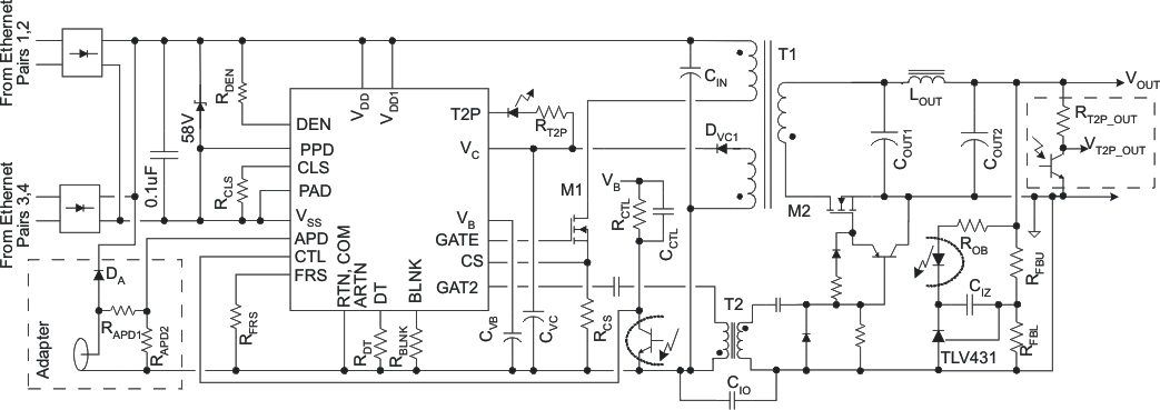
9.2 Typical Application
 Figure 27. Driven Synchronous Flyback