JAJSER5A February 2018 – April 2018 LMK05028
PRODUCTION DATA.
- 1 特長
- 2 アプリケーション
- 3 概要
- 4 改訂履歴
- 5 概要(続き)
- 6 Pin Configuration and Functions
- 7 Specifications
- 8 Parameter Measurement Information
-
9 Detailed Description
- 9.1 Overview
- 9.2 Functional Block Diagrams
- 9.3
Feature Description
- 9.3.1 Oscillator Input (XO_P/N)
- 9.3.2 TCXO/OCXO Input (TCXO_IN)
- 9.3.3 Reference Inputs (INx_P/N)
- 9.3.4 Clock Input Interfacing and Termination
- 9.3.5 Reference Input Mux Selection
- 9.3.6 Hitless Switching
- 9.3.7 Gapped Clock Support on Reference Inputs
- 9.3.8 Input Clock and PLL Monitoring, Status, and Interrupts
- 9.3.9
PLL Channels
- 9.3.9.1 PLL Frequency Relationships
- 9.3.9.2 Analog PLL (APLL)
- 9.3.9.3 APLL XO Doubler
- 9.3.9.4 APLL Phase Frequency Detector (PFD) and Charge Pump
- 9.3.9.5 APLL Loop Filter
- 9.3.9.6 APLL Voltage Controlled Oscillator (VCO)
- 9.3.9.7 APLL VCO Post-Dividers (P1, P2)
- 9.3.9.8 APLL Fractional N Divider (N) With SDM
- 9.3.9.9 REF-DPLL Reference Divider (R)
- 9.3.9.10 TCXO/OCXO Input Doubler and M Divider
- 9.3.9.11 TCXO Mux
- 9.3.9.12 REF-DPLL and TCXO-DPLL Time-to-Digital Converter (TDC)
- 9.3.9.13 REF-DPLL and TCXO-DPLL Loop Filter
- 9.3.9.14 REF-DPLL and TCXO-DPLL Feedback Dividers
- 9.3.10 Output Clock Distribution
- 9.3.11 Output Channel Muxes
- 9.3.12 Output Dividers
- 9.3.13 Clock Outputs (OUTx_P/N)
- 9.3.14 Glitchless Output Clock Start-Up
- 9.3.15 Clock Output Interfacing and Termination
- 9.3.16 Output Synchronization (SYNC)
- 9.3.17 Zero-Delay Mode (ZDM) Configuration
- 9.3.18 PLL Cascading With Internal VCO Loopback
- 9.4 Device Functional Modes
- 9.5 Programming
- 9.6 Register Maps
- 10Application and Implementation
- 11Power Supply Recommendations
- 12Layout
- 13デバイスおよびドキュメントのサポート
- 14メカニカル、パッケージ、および注文情報
9.3.3 Reference Inputs (INx_P/N)
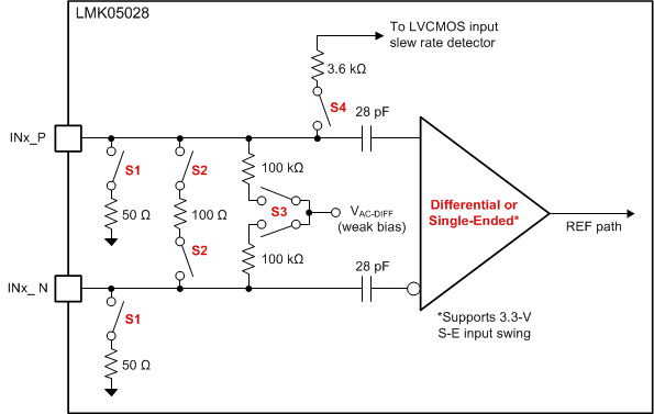
The reference inputs (IN0 to IN3) can accept differential or single-ended clocks to synchronize any of the PLL channels. Each input has programmable input type, termination, and AC-coupled input biasing configurations as shown in Figure 26. Each input buffer drives the reference input mux of both DPLL blocks. The DPLL input mux can select from any of the reference inputs. Any DPLL can switch between inputs with different frequencies provided they can be divided-down to a common frequency by DPLL R dividers (DPLLy_REFx_RDIV). The reference input paths also drive the various detector blocks for reference input monitoring and validation. The selected reference of each DPLL input (before the R divider) can be routed through the TCXO/Ref bypass mux and output muxes, allowing a buffered copy of either DPLL reference input on OUT0 and/or OUT1.
 Figure 26. Reference Input Buffer
 Table 5 lists the reference input buffer configurations for common clock interface types.
Table 5. Reference Input Buffer Modes
| REFx_TYPE | INPUT TYPES | INTERNAL SWITCH SETTINGS | ||
|---|---|---|---|---|
| INTERNAL TERM.
(S1, S2)(1) |
INTERNAL BIAS
(S3)(2) |
LVCMOS SLEW RATE DETECT (S4)(3) | ||
| 0h | LVDS, CML, LVPECL
(DC-coupled) |
OFF | OFF | OFF |
| 1h | LVDS, CML, LVPECL
(AC-coupled) |
OFF | ON (1.3 V) | OFF |
| 3h | LVDS, CML, LVPECL
(AC-coupled, internal 100-Ω) |
100 Ω | ON (1.3 V) | OFF |
| 4h | HCSL
(DC-coupled, internal 50-Ω) |
50 Ω | OFF | OFF |
| 8h | LVCMOS | OFF | OFF | ON |