JAJSES9 February 2018 DAC8771
PRODUCTION DATA.
- 1 特長
- 2 アプリケーション
- 3 概要
- 4 改訂履歴
- 5 Device Comparison Table
- 6 Pin Configuration and Functions
- 7 Specifications
-
8 Detailed Description
- 8.1 Overview
- 8.2 Functional Block Diagram
- 8.3
Feature Description
- 8.3.1 Current Output Stage
- 8.3.2 Voltage Output Stage
- 8.3.3 Buck-Boost Converter
- 8.3.4 Analog Power Supply
- 8.3.5 Digital Power Supply
- 8.3.6 Internal Reference
- 8.3.7 Power-On-Reset
- 8.3.8 ALARM Pin
- 8.3.9 Power GOOD bit
- 8.3.10 Status Register
- 8.3.11 Status Mask
- 8.3.12 Alarm Action
- 8.3.13 Watchdog Timer
- 8.3.14 Programmable Slew Rate
- 8.3.15 HART Interface
- 8.4 Device Functional Modes
- 8.5
Register Maps
- 8.5.1
Register Maps
- 8.5.1.1 DAC8771 Commands
- 8.5.1.2
Register Maps and Bit Functions
- 8.5.1.2.1 No Operation Register (address = 0x00) [reset = 0x0000]
- 8.5.1.2.2 Reset Register (address = 0x01) [reset = 0x0000]
- 8.5.1.2.3 Reset Config Register (address = 0x02) [reset = 0x0000]
- 8.5.1.2.4 Select DAC Register (address = 0x03) [reset = 0x0000]
- 8.5.1.2.5 Configuration DAC Register (address = 0x04) [reset = 0x0000]
- 8.5.1.2.6 DAC Data Register (address = 0x05) [reset = 0x0000]
- 8.5.1.2.7 Select Buck-Boost Converter Register (address = 0x06) [reset = 0x0000]
- 8.5.1.2.8 Configuration Buck-Boost Register (address = 0x07) [reset = 0x0000]
- 8.5.1.2.9 DAC Channel Calibration Enable Register (address = 0x08) [reset = 0x0000]
- 8.5.1.2.10 DAC Channel Gain Calibration Register (address = 0x09) [reset = 0x0000]
- 8.5.1.2.11 DAC Channel Offset Calibration Register (address = 0x0A) [reset = 0x0000]
- 8.5.1.2.12 Status Register (address = 0x0B) [reset = 0x1000]
- 8.5.1.2.13 Status Mask Register (address = 0x0C) [reset = 0x0000]
- 8.5.1.2.14 Alarm Action Register (address = 0x0D) [reset = 0x0000]
- 8.5.1.2.15 User Alarm Code Register (address = 0x0E) [reset = 0x0000]
- 8.5.1.2.16 Reserved Register (address = 0x0F) [reset = N/A]
- 8.5.1.2.17 Write Watchdog Timer Register (address = 0x10) [reset = 0x0000]
- 8.5.1.2.18 Reserved Register (address 0x12 - 0xFF) [reset = N/A]
- 8.5.1
Register Maps
- 9 Application and Implementation
- 10Power Supply Recommendations
- 11Layout
- 12デバイスおよびドキュメントのサポート
- 13メカニカル、パッケージ、および注文情報
8.3.3 Buck-Boost Converter
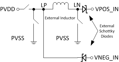
The DAC8771 includes a Buck-Boost Converter to minimize the power dissipation of the chip and provides significant system integration. This Buck-Boost converter is based on a Single Inductor Multiple Output (SIMO) architecture and requires a single inductor to simultaneously generate all the analog power supplies required by the chip. The Buck-Boost converter uses three on-chip switches (shown in Figure 99) which are synchronously controlled via current mode control logic. The DC/DC converter is designed to work in discontinuous conduction mode (DCM) with an external inductor of value 100 µH connected between LN and LP pins (see Buck-Boost Converter External Component Selection section). The peak inductor current inductor is limited to a value of 0.5 A internally.
 Figure 99. Buck-Boost Converter
The Buck-Boost converter employs a variable switching frequency technique. This technique increases the converter efficiency at all loads by automatically reducing the switching frequency at light loads and increasing it at heavy loads. At no load condition, the converter stops switching completely until the load capacitor discharges by a preset voltage. At this point, the converter automatically starts switching and recharges the load capacitor(s). In addition to saving power at all loads, this technique ensures low switching noise on the converter outputs at light loads. The minimum load capacitor for the Buck-Boost converter is 10 µF. This capacitor must be connected between the Schottky diode(s) and ground (0 V) for each arm of the Buck-Boost converter. The Buck-Boost converter, when enabled, generates ripples on the supply pins (VPOS_IN and VNEG_IN). This ripple is typically attenuated by the power supply rejection ratio of the output amplifiers (IOUT or VOUT) and appears as noise on the output pin of the amplifiers (IOUT and VOUT). A larger load capacitor in combination with additional filter (see application section) reduces the output ripple at the expense of increasing settling time of the converter output.
The input voltage to the Buck-Boost converter (pin PVDD) can vary from +12 V to +36 V. These outputs can be individually enabled or disabled via the user SPI interface (See Commands in Table 4 and Table 5).