JAJSET7C May   2017  – October 2018 IWR1443

PRODUCTION DATA.  

  1. 1デバイスの概要
    1. 1.1 特長
    2. 1.2 アプリケーション
    3. 1.3 概要
    4. 1.4 機能ブロック図
  2. 2改訂履歴
  3. 3Device Comparison
    1. 3.1 Related Products
  4. 4Terminal Configuration and Functions
    1. 4.1 Pin Diagram
    2. 4.2 Signal Descriptions
      1. Table 4-1 Signal Descriptions
    3. 4.3 Pin Multiplexing
  5. 5Specifications
    1. 5.1 Absolute Maximum Ratings
    2. 5.2 ESD Ratings
    3. 5.3 Power-On Hours (POH)
    4. 5.4 Recommended Operating Conditions
    5. 5.5 Power Supply Specifications
    6. 5.6 Power Consumption Summary
    7. 5.7 RF Specification
    8. 5.8 Thermal Resistance Characteristics for FCBGA Package [ABL0161]
    9. 5.9 Timing and Switching Characteristics
      1. 5.9.1  Power Supply Sequencing and Reset Timing
      2. 5.9.2  Synchronized Frame Triggering
      3. 5.9.3  Input Clocks and Oscillators
        1. 5.9.3.1 Clock Specifications
      4. 5.9.4  Multibuffered / Standard Serial Peripheral Interface (MibSPI)
        1. 5.9.4.1 Peripheral Description
        2. 5.9.4.2 MibSPI Transmit and Receive RAM Organization
          1. Table 5-8  SPI Timing Conditions
          2. Table 5-9  SPI Master Mode Switching Parameters (CLOCK PHASE = 0, SPICLK = output, SPISIMO = output, and SPISOMI = input)
          3. Table 5-10 SPI Master Mode Switching Parameters (CLOCK PHASE = 1, SPICLK = output, SPISIMO = output, and SPISOMI = input)
        3. 5.9.4.3 SPI Slave Mode I/O Timings
          1. Table 5-11 SPI Slave Mode Switching Parameters (SPICLK = input, SPISIMO = input, and SPISOMI = output)
        4. 5.9.4.4 Typical Interface Protocol Diagram (Slave Mode)
      5. 5.9.5  LVDS Interface Configuration
        1. 5.9.5.1 LVDS Interface Timings
      6. 5.9.6  General-Purpose Input/Output
        1. Table 5-13 Switching Characteristics for Output Timing versus Load Capacitance (CL)
      7. 5.9.7  Controller Area Network Interface (DCAN)
        1. Table 5-14 Dynamic Characteristics for the DCANx TX and RX Pins
      8. 5.9.8  Serial Communication Interface (SCI)
        1. Table 5-15 SCI Timing Requirements
      9. 5.9.9  Inter-Integrated Circuit Interface (I2C)
        1. Table 5-16 I2C Timing Requirements
      10. 5.9.10 Quad Serial Peripheral Interface (QSPI)
        1. Table 5-17 QSPI Timing Conditions
        2. Table 5-18 Timing Requirements for QSPI Input (Read) Timings
        3. Table 5-19 QSPI Switching Characteristics
      11. 5.9.11 JTAG Interface
        1. Table 5-20 JTAG Timing Conditions
        2. Table 5-21 Timing Requirements for IEEE 1149.1 JTAG
        3. Table 5-22 Switching Characteristics Over Recommended Operating Conditions for IEEE 1149.1 JTAG
      12. 5.9.12 Camera Serial Interface (CSI)
        1. Table 5-23 CSI Switching Characteristics
  6. 6Detailed Description
    1. 6.1 Overview
    2. 6.2 Functional Block Diagram
    3. 6.3 External Interfaces
    4. 6.4 Subsystems
      1. 6.4.1 RF and Analog Subsystem
        1. 6.4.1.1 Clock Subsystem
        2. 6.4.1.2 Transmit Subsystem
        3. 6.4.1.3 Receive Subsystem
        4. 6.4.1.4 Radio Processor Subsystem
      2. 6.4.2 Master (Control) System
      3. 6.4.3 Host Interface
    5. 6.5 Accelerators and Coprocessors
    6. 6.6 Other Subsystems
      1. 6.6.1 A2D Data Format Over CSI2 Interface
      2. 6.6.2 ADC Channels (Service) for User Application
        1. Table 6-2 GP-ADC Parameter
    7. 6.7 Identification
    8. 6.8 Boot Modes
      1. 6.8.1 Flashing Mode
      2. 6.8.2 Functional Mode
  7. 7Applications, Implementation, and Layout
    1. 7.1 Application Information
    2. 7.2 Reference Schematic
    3. 7.3 Layout
      1. 7.3.1 Layout Guidelines
      2. 7.3.2 Layout Example
      3. 7.3.3 Stackup Details
  8. 8Device and Documentation Support
    1. 8.1 Device Nomenclature
    2. 8.2 Tools and Software
    3. 8.3 Documentation Support
    4. 8.4 Community Resources
    5. 8.5 商標
    6. 8.6 静電気放電に関する注意事項
    7. 8.7 Export Control Notice
    8. 8.8 Glossary
  9. 9Mechanical, Packaging, and Orderable Information
    1. 9.1 Packaging Information

Power Supply Sequencing and Reset Timing

The IWR1443 device expects all external voltage rails to be stable before reset is deasserted. Figure 5-2 describes the device wake-up sequence.
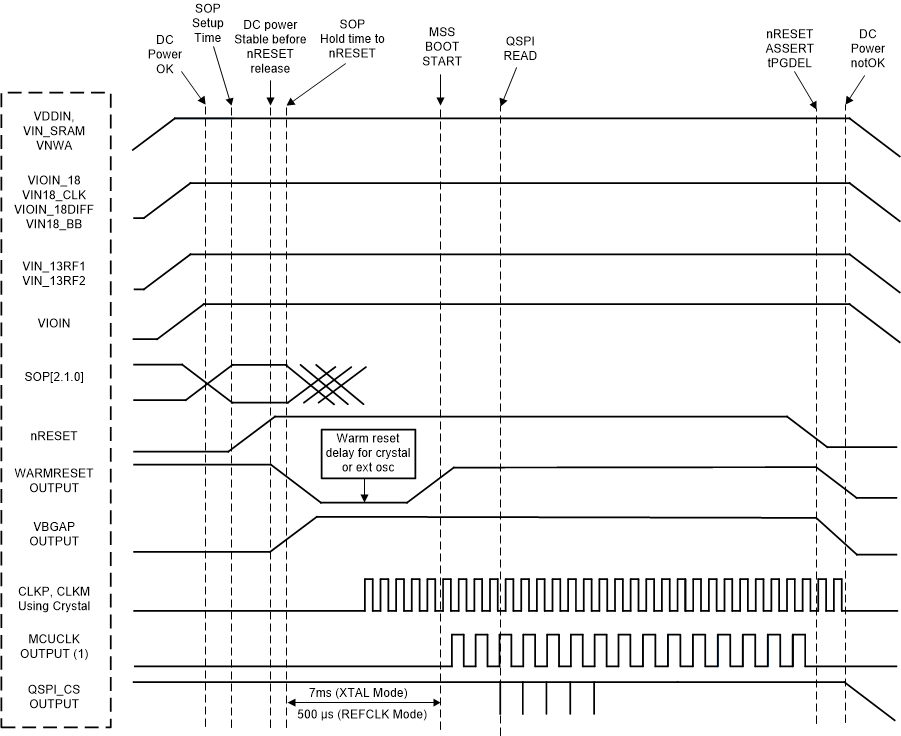
IWR1443 device_wakeup_seq_c_iwr14.gif
MCU_CLK_OUT in autonomous mode, where IWR1443 application is booted from the serial flash, MCU_CLK_OUT is not enabled by default by the device bootloader.
Figure 5-2 Device Wake-up Sequence