JAJSF07A March   2018  – November 2018 LMX8410L

PRODUCTION DATA.  

  1. 特長
  2. アプリケーション
  3. 概要
    1.     Device Images
      1.      ブロック概略図
  4. 改訂履歴
  5. Pin Configuration and Functions
    1.     Pin Functions
  6. Specifications
    1. 6.1 Absolute Maximum Ratings
    2. 6.2 ESD Ratings
    3. 6.3 Recommended Operating Conditions
    4. 6.4 Thermal Information
    5. 6.5 Electrical Characteristics
    6. 6.6 Timing Requirements
    7. 6.7 Typical Characteristics
  7. Detailed Description
    1. 7.1 Overview
    2. 7.2 Functional Block Diagram
    3. 7.3 Feature Description
      1. 7.3.1 Device Configurations and Feature Description
        1. 7.3.1.1 RF, LO and IF Interfaces
          1. 7.3.1.1.1 RF Interface
          2. 7.3.1.1.2 LO Interface
            1. 7.3.1.1.2.1 LO Interface as Output Port
            2. 7.3.1.1.2.2 LO Interface as Input Port
          3. 7.3.1.1.3 Baseband Interface
        2. 7.3.1.2 Device Configurations Overview
          1. 7.3.1.2.1 Initialize the Device
          2. 7.3.1.2.2 Configure LO Modes
          3. 7.3.1.2.3 Set Up External LO Clock
          4. 7.3.1.2.4 Perform DCOC (DC Offset Correction)
          5. 7.3.1.2.5 Turn Off SM Clock
          6. 7.3.1.2.6 Perform IMRR (Image Rejection Ratio) Calibration
        3. 7.3.1.3 State Machine Clock
          1. 7.3.1.3.1 Set Divider Values For Internal LO Mode
          2. 7.3.1.3.2 Set Divider Values For External LO Mode
        4. 7.3.1.4 DCOC (DC Offset Correction)
          1. 7.3.1.4.1 RF Input Power Restriction During DCOC
          2. 7.3.1.4.2 Set Up DCOC Clock Divider
        5. 7.3.1.5 Image Rejection Calibration
          1. 7.3.1.5.1 Phase Calibration
          2. 7.3.1.5.2 Gain Calibration
        6. 7.3.1.6 IF Amplifier Common Mode Configurations
        7. 7.3.1.7 Synchronization Mode (Internal LO Mode Only)
          1. 7.3.1.7.1 Synchronization of the LO_OUT Output to the Fosc Input
          2. 7.3.1.7.2 Synchronization of I/Q Outputs to Fosc Inputs Using Internal LO
    4. 7.4 Device Functional Modes
      1. 7.4.1 Internal LO Mode
        1. 7.4.1.1 VCO Range Uncertainty for 7.5 to 7.7 GHz
      2. 7.4.2 External LO Mode
    5. 7.5 Programming
      1. 7.5.1 General Comments Regarding Programming
      2. 7.5.2 Recommended Initial Power Up Sequence
      3. 7.5.3 Recommended and Power on Reset Bit Values
    6. 7.6 Register Map
      1. 7.6.1  R0 Register (Address = 0x0) [reset = X]
        1. Table 9. R0 Register Field Descriptions
      2. 7.6.2  R1 Register (Address = 0x1) [reset = 0x3]
        1. Table 10. R1 Register Field Descriptions
      3. 7.6.3  R2 Register (Address = 0x2) [reset = X]
        1. Table 11. R2 Register Field Descriptions
      4. 7.6.4  R9 Register (Address = 0x9) [reset = X]
        1. Table 12. R9 Register Field Descriptions
      5. 7.6.5  R10 Register (Address = 0xA) [reset = 0x80]
        1. Table 13. R10 Register Field Descriptions
      6. 7.6.6  R11 Register (Address = 0xB) [reset = 0x10]
        1. Table 14. R11 Register Field Descriptions
      7. 7.6.7  R14 Register (Address = 0xE) [reset = 0x70]
        1. Table 15. R14 Register Field Descriptions
      8. 7.6.8  R36 Register (Address = 0x24) [reset = 0x64]
        1. Table 16. R36 Register Field Descriptions
      9. 7.6.9  R37 Register (Address = 0x25) [reset = 0x200]
        1. Table 17. R37 Register Field Descriptions
      10. 7.6.10 R38 Register (Address = 0x26) [reset = 0x0]
        1. Table 18. R38 Register Field Descriptions
      11. 7.6.11 R39 Register (Address = 0x27) [reset = 0x2710]
        1. Table 19. R39 Register Field Descriptions
      12. 7.6.12 R40 Register (Address = 0x28) [reset = 0x0]
        1. Table 20. R40 Register Field Descriptions
      13. 7.6.13 R41 Register (Address = 0x29) [reset = 0x0]
        1. Table 21. R41 Register Field Descriptions
      14. 7.6.14 R42 Register (Address = 0x2A) [reset = 0x0]
        1. Table 22. R42 Register Field Descriptions
      15. 7.6.15 R43 Register (Address = 0x2B) [reset = 0x0]
        1. Table 23. R43 Register Field Descriptions
      16. 7.6.16 R44 Register (Address = 0x2C) [reset = 0xA2]
        1. Table 24. R44 Register Field Descriptions
      17. 7.6.17 R46 Register (Address = 0x2E) [reset = 0x1]
        1. Table 25. R46 Register Field Descriptions
      18. 7.6.18 R58 Register (Address = 0x3A) [reset = 0x8000]
        1. Table 26. R58 Register Field Descriptions
      19. 7.6.19 R59 Register (Address = 0x3B) [reset = 0x1]
        1. Table 27. R59 Register Field Descriptions
      20. 7.6.20 R69 Register (Address = 0x45) [reset = 0x0]
        1. Table 28. R69 Register Field Descriptions
      21. 7.6.21 R70 Register (Address = 0x46) [reset = 0xC350]
        1. Table 29. R70 Register Field Descriptions
      22. 7.6.22 R75 Register (Address = 0x4B) [reset = 0x0]
        1. Table 30. R75 Register Field Descriptions
      23. 7.6.23 R78 Register (Address = 0x4E) [reset = 0x0]
        1. Table 31. R78 Register Field Descriptions
      24. 7.6.24 R79 Register (Address = 0x4F) [reset = 0x7000]
        1. Table 32. R79 Register Field Descriptions
      25. 7.6.25 R80 Register (Address = 0x50) [reset = 0xA]
        1. Table 33. R80 Register Field Descriptions
      26. 7.6.26 R81 Register (Address = 0x51) [reset = 0x0]
        1. Table 34. R81 Register Field Descriptions
      27. 7.6.27 R82 Register (Address = 0x52) [reset = 0x23]
        1. Table 35. R82 Register Field Descriptions
      28. 7.6.28 R83 Register (Address = 0x53) [reset = 0x2000]
        1. Table 36. R83 Register Field Descriptions
      29. 7.6.29 R84 Register (Address = 0x54) [reset = 0x1900]
        1. Table 37. R84 Register Field Descriptions
      30. 7.6.30 R88 Register (Address = 0x58) [reset = 0x0]
        1. Table 38. R88 Register Field Descriptions
      31. 7.6.31 R94 Register (Address = 0x5E) [reset = 0x8080]
        1. Table 39. R94 Register Field Descriptions
      32. 7.6.32 R95 Register (Address = 0x5F) [reset = X]
        1. Table 40. R95 Register Field Descriptions
      33. 7.6.33 R103 Register (Address = 0x67) [reset = X]
        1. Table 41. R103 Register Field Descriptions
      34. 7.6.34 R110 Register (Address = 0x6E) [reset = X]
        1. Table 42. R110 Register Field Descriptions
      35. 7.6.35 R111 Register (Address = 0x6F) [reset = 0x0]
        1. Table 43. R111 Register Field Descriptions
      36. 7.6.36 R112 Register (Address = 0x70) [reset = 0x0]
        1. Table 44. R112 Register Field Descriptions
      37. 7.6.37 R121 Register (Address = 0x79) [reset = 0x0]
        1. Table 45. R121 Register Field Descriptions
      38. 7.6.38 R123 Register (Address = 0x7B) [reset = 0x3]
        1. Table 46. R123 Register Field Descriptions
      39. 7.6.39 R126 Register (Address = 0x7E) [reset = X]
        1. Table 47. R126 Register Field Descriptions
  8. Application and Implementation
    1. 8.1 Application Information
    2. 8.2 Typical Application
      1. 8.2.1 Design Requirements
      2. 8.2.2 Detailed Design Procedure
      3. 8.2.3 Application Curve
  9. Power Supply Recommendations
  10. 10Layout
    1. 10.1 Layout Guidelines
      1. 10.1.1 High Frequency Trace Routing
      2. 10.1.2 Power Trace Routing
    2. 10.2 Layout Examples
  11. 11デバイスおよびドキュメントのサポート
    1. 11.1 ドキュメントのサポート
      1. 11.1.1 関連資料
    2. 11.2 ドキュメントの更新通知を受け取る方法
    3. 11.3 コミュニティ・リソース
    4. 11.4 商標
    5. 11.5 静電気放電に関する注意事項
    6. 11.6 Glossary
  12. 12メカニカル、パッケージ、および注文情報

Typical Characteristics

LMX8410L D001_SNAS730.gif
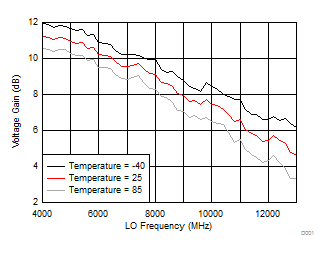
Figure 3. Voltage Gain Across LO Frequency for Internal LO Mode
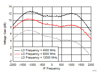
LMX8410L D003_SNAS730.gif
Figure 5. Voltage Gain Across IF Frequency for Internal LO Mode
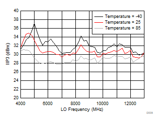
LMX8410L D005_SNAS730.gif
Figure 7. IIP3 Across LO Frequency for Internal LO Mode
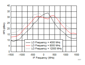
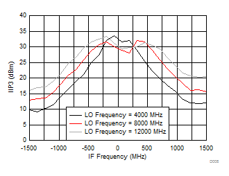
LMX8410L D007_SNAS730.gif
Figure 9. IIP3 Across IF Frequency for Internal LO Mode
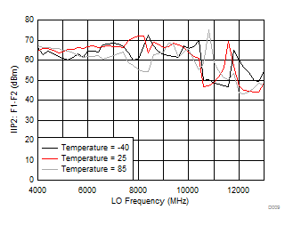
LMX8410L D009_SNAS730.gif
Figure 11. IIP2: F1-F2 Across LO Frequency for Internal LO Mode
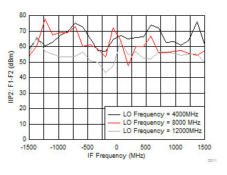
LMX8410L D011_SNAS730.gif
Figure 13. IIP2: F1-F2 Across IF Frequency for Internal LO Mode
LMX8410L D013_SNAS730.gif
Figure 15. IIP2: F1+F2 Across LO Frequency for Internal LO Mode
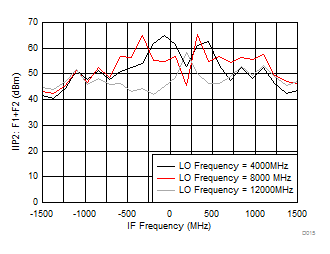
LMX8410L D015_SNAS730.gif
Figure 17. IIP2: F1+F2 Across IF Frequency for Internal LO Mode
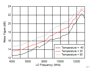
LMX8410L D017_SNAS730.gif
Figure 19. Noise Figure Across LO Frequency for Internal LO Mode
LMX8410L D019_SNAS730.gif
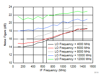
Figure 21. Noise Figure Across IF Frequency for Internal LO Mode
LMX8410L D022_SNAS730.gif
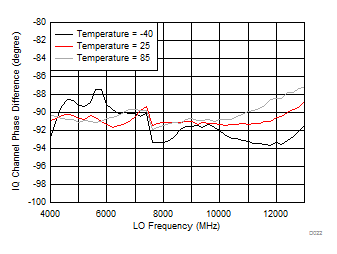
Figure 23. Uncalibrated IQ Phase Difference for Internal LO Mode
LMX8410L D025_SNAS730.gif
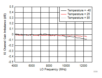
Figure 25. Uncalibrated IQ Gain Imbalance for Internal LO Mode
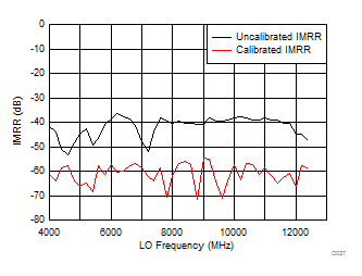
LMX8410L D027_SNAS730.gif
Figure 27. IMRR for Internal LO Mode: Calibrated and Uncalibrated
LMX8410L D040_SNAS730.gif
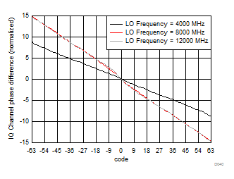
Minus sign on x-axis means polarity is set to '1'.
Figure 29. IMRR Phase Calibration: Fine Accuracy Mode
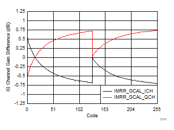
LMX8410L D045_SNAS730.gif
Figure 31. IMRR Gain Calibration
LMX8410L D030_SNAS730.gif
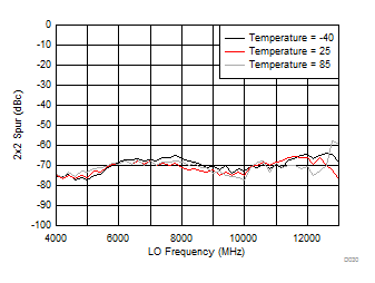
Figure 33. 2x2 Spur for External LO Mode
LMX8410L D032_SNAS730.gif
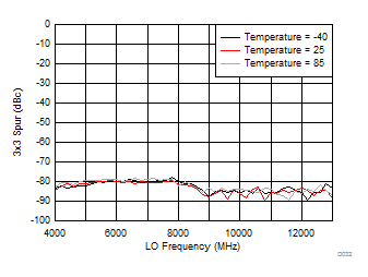
Figure 35. 3x3 Spur for External LO Mode
LMX8410L D034_SNAS730.gif
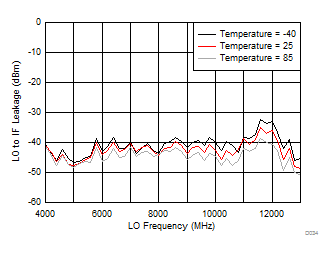
Figure 37. LO to IF Leakage Level
LMX8410L D036_SNAS730.gif
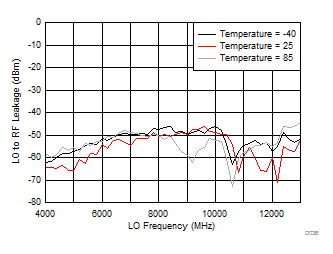
Figure 39. LO to RF Leakage Level: External LO Mode
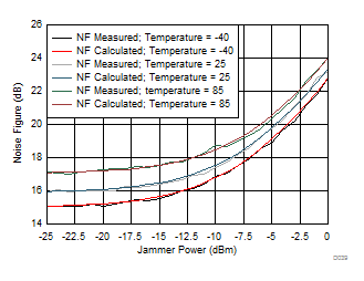
LMX8410L D039_SNAS730.gif
  1. Jammer frequency = 8.8GHz, LO = 7.8GHz, IF = 100MHz.
  2. Internal LO phase noise values used for calculation at -40, 25, and 85 degrees C are –155, –154.5 and –154 dBc/Hz, separately.
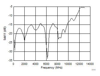
Figure 41. Noise Figure with Jammer
LMX8410L D043_SNAS730.gif
Figure 43. LO Port Mixed Modes S11
LMX8410L D002_SNAS730.gif
Figure 4. Voltage Gain Across LO frequency for External LO Mode
LMX8410L D004_SNAS730.gif
Figure 6. Voltage Gain Across IF Frequency for External LO Mode
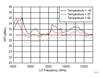
LMX8410L D006_SNAS730.gif
Figure 8. IIP3 Across LO Frequency for External LO Mode
LMX8410L D008_SNAS730.gif
Figure 10. IIP3 Across IF Frequency for External LO Mode
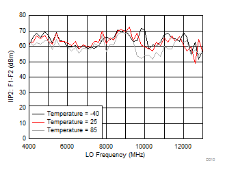
LMX8410L D010_SNAS730.gif
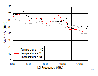
Figure 12. IIP2: F1-F2 Across LO Frequency for External LO Mode
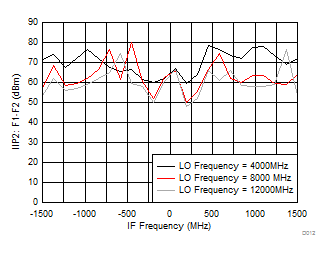
LMX8410L D012_SNAS730.gif
Figure 14. IIP2: F1-F2 Across IF Frequency for External LO Mode
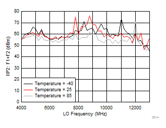
LMX8410L D014_SNAS730.gif
Figure 16. IIP2: F1+F2 Across LO Frequency for External LO Mode
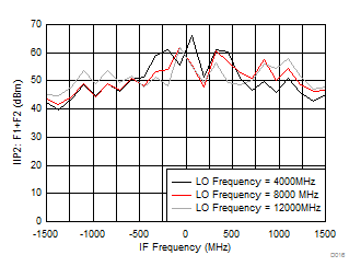
LMX8410L D016_SNAS730.gif
Figure 18. IIP2: F1+F2 Across IF Frequency for External LO Mode
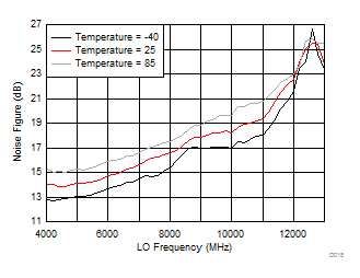
LMX8410L D018_SNAS730.gif
Figure 20. Noise Figure Across LO Frequency for External LO Mode
LMX8410L D020_SNAS730.gif
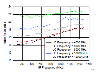
Figure 22. Noise Figure Across IF Frequency for External LO Mode
LMX8410L D024_SNAS730.gif
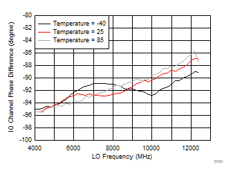
Figure 24. Uncalibrated IQ Phase Difference for External LO Mode
LMX8410L D026_SNAS730.gif
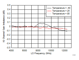
Figure 26. Uncalibrated IQ Gain Imbalance for External LO Mode
LMX8410L D028_SNAS730.gif
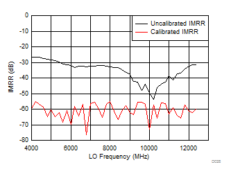
Figure 28. IMRR for External LO Mode: Calibrated and Uncalibrated
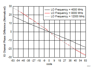
LMX8410L D041_SNAS730.gif
Figure 30. IMRR Phase Calibration: Extended Range Mode
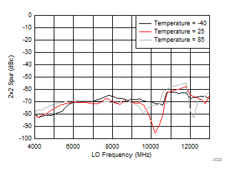
LMX8410L D029_SNAS730.gif
Figure 32. 2x2 Spur for Internal LO Mode
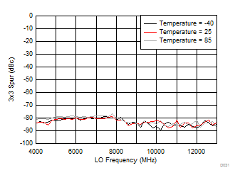
LMX8410L D031_SNAS730.gif
Figure 34. 3x3 Spur for Internal LO Mode
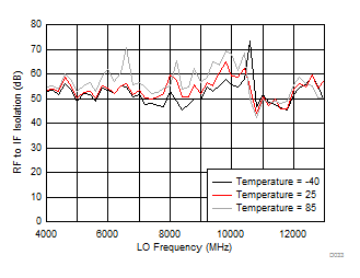
LMX8410L D033_SNAS730.gif
Figure 36. RF to IF Isolation
LMX8410L D035_SNAS730.gif
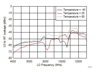
Figure 38. LO to RF Leakage Level: Internal LO Mode
LMX8410L D037_SNAS730.gif
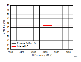
  1. The LO frequency is capped at 6600MHz because IP1dB exceeds +10dBm when LO frequency goes beyond 6600MHz; The device can be damaged when input power is more than +10dBm.
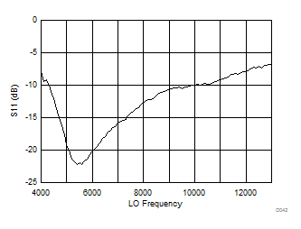
Figure 40. OP1dB Across LO Frequency
LMX8410L D042_SNAS730.gif
Figure 42. RF Port S11
LMX8410L D044_SNAS730.gif
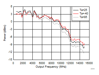
  1. Board losses and mismatch are not subtracted out. True output power may be higher. This plot shows single-ended LO output power only. Differential output power can be higher.
Figure 44. LO Output Power
Measurements are done at 25 degree C unless temperature is specified in the plots.
For measurements across LO frequency, IF = 65MHz, and LO injection type is high side injection. For measurements across IF frequency, high side injection is applied
For all measurements that require RF input, RF input power = -10 dBm unless otherwise specified.
For two-tone measurements, the separation between two tones is 17MHz.
For all measurements, internal 1.7V VCM is applied.
For all external LO mode measurements, LO power = +6 dBm.
IF baluns used for measurements are: ADT2-18+ from Mini-Circuits™.
LO balun used for measurements is: BIB-100G from PPM-Test™.
RF combiner used for measurements of IP2, IP3 and NF with jammer is: 4426-2 from Narda-MITEQ™.
All path losses are calibrated out.