JAJSF23B March   2018  – July 2018 INA1620

PRODUCTION DATA.  

  1. 特長
  2. アプリケーション
  3. 概要
    1.     Device Images
      1.      INA1620の簡略化された内部回路図
      2.      FFT: 1kHz、32Ω負荷、50mW
  4. 改訂履歴
  5. Pin Configuration and Functions
    1.     Pin Functions
  6. Specifications
    1. 6.1 Absolute Maximum Ratings
    2. 6.2 ESD Ratings
    3. 6.3 Recommended Operating Conditions
    4. 6.4 Thermal Information
    5. 6.5 Electrical Characteristics:
    6. 6.6 Typical Characteristics
  7. Detailed Description
    1. 7.1 Overview
    2. 7.2 Functional Block Diagram
    3. 7.3 Feature Description
      1. 7.3.1 Matched Thin-Film Resistor Pairs
      2. 7.3.2 Power Dissipation
      3. 7.3.3 Thermal Shutdown
      4. 7.3.4 EN Pin
      5. 7.3.5 GND Pin
      6. 7.3.6 Input Protection
    4. 7.4 Device Functional Modes
      1. 7.4.1 Shutdown Mode
      2. 7.4.2 Output Transients During Power Up and Power Down
  8. Application and Implementation
    1. 8.1 Application Information
      1. 8.1.1 Noise Performance
      2. 8.1.2 Resistor Tolerance
      3. 8.1.3 EMI Rejection
      4. 8.1.4 EMIRR +IN Test Configuration
    2. 8.2 Typical Application
      1. 8.2.1 Design Requirements
      2. 8.2.2 Detailed Design Procedure
      3. 8.2.3 Application Curves
    3. 8.3 Other Application Examples
      1. 8.3.1 Preamplifier for Professional Microphones
  9. Power Supply Recommendations
  10. 10Layout
    1. 10.1 Layout Guidelines
    2. 10.2 Layout Example
  11. 11デバイスおよびドキュメントのサポート
    1. 11.1 デバイス・サポート
      1. 11.1.1 開発サポート
        1. 11.1.1.1 TINA-TI(無料のダウンロード・ソフトウェア)
        2. 11.1.1.2 TI Precision Designs
    2. 11.2 ドキュメントのサポート
      1. 11.2.1 関連資料
    3. 11.3 ドキュメントの更新通知を受け取る方法
    4. 11.4 コミュニティ・リソース
    5. 11.5 商標
    6. 11.6 静電気放電に関する注意事項
    7. 11.7 Glossary
  12. 12メカニカル、パッケージ、および注文情報

Resistor Tolerance

The INA1620 integrated resistor pairs use an advanced thin film process to create resistor pairs that have excellent matching. Each specific resistor pair is specifically designed for accurate matching between the two resistors. Figure 42 shows the distribution of resistor matching for a typical device population. The equation used to calculate matching between resistors in a pair is shown in Equation 5.

Equation 5. INA1620 eq5a_sbos859.gif

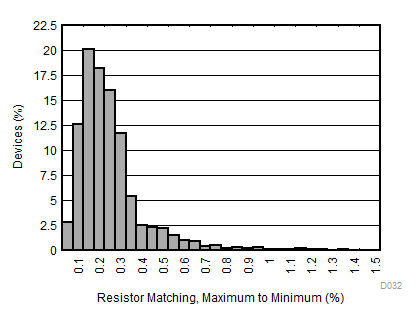
In addition to excellent matching between resistors in each resistor pair, all resistors on a single INA1620 achieve good matching due to inherent process matching across each device. Figure 52 shows a typical distribution of the worst-case matching across all resistors on a single INA1620. The matching was calculated using the highest value resistance on a device matched with the lowest resistance value on the same device.
INA1620 D032.gifFigure 52. Matching Histogram, Maximum to Minimum