JAJSF69A April   2018  – October 2018 ADS112C04

PRODUCTION DATA.  

  1. 特長
  2. アプリケーション
  3. 概要
    1.     Device Images
      1.      Kタイプ熱電対温度の測定
  4. 概要(続き)
  5. 改訂履歴
  6. Pin Configuration and Functions
    1.     Pin Functions
  7. Specifications
    1. 7.1 Absolute Maximum Ratings
    2. 7.2 ESD Ratings
    3. 7.3 Recommended Operating Conditions
    4. 7.4 Thermal Information
    5. 7.5 Electrical Characteristics
    6. 7.6 I2C Timing Requirements
    7. 7.7 I2C Switching Characteristics
    8. 7.8 Typical Characteristics
  8. Parameter Measurement Information
    1. 8.1 Noise Performance
  9. Detailed Description
    1. 9.1 Overview
    2. 9.2 Functional Block Diagram
    3. 9.3 Feature Description
      1. 9.3.1  Multiplexer
      2. 9.3.2  Low-Noise Programmable Gain Stage
        1. 9.3.2.1 PGA Input Voltage Requirements
        2. 9.3.2.2 Bypassing the PGA
      3. 9.3.3  Voltage Reference
      4. 9.3.4  Modulator and Internal Oscillator
      5. 9.3.5  Digital Filter
      6. 9.3.6  Conversion Times
      7. 9.3.7  Excitation Current Sources
      8. 9.3.8  Sensor Detection
      9. 9.3.9  System Monitor
      10. 9.3.10 Temperature Sensor
        1. 9.3.10.1 Converting From Temperature to Digital Codes
          1. 9.3.10.1.1 For Positive Temperatures (For Example, 50°C):
          2. 9.3.10.1.2 For Negative Temperatures (For Example, –25°C):
        2. 9.3.10.2 Converting From Digital Codes to Temperature
      11. 9.3.11 Offset Calibration
      12. 9.3.12 Conversion Data Counter
      13. 9.3.13 Data Integrity Features
    4. 9.4 Device Functional Modes
      1. 9.4.1 Power-Up and Reset
        1. 9.4.1.1 Power-On Reset
        2. 9.4.1.2 RESET Pin
        3. 9.4.1.3 Reset by Command
      2. 9.4.2 Conversion Modes
        1. 9.4.2.1 Single-Shot Conversion Mode
        2. 9.4.2.2 Continuous Conversion Mode
      3. 9.4.3 Operating Modes
        1. 9.4.3.1 Normal Mode
        2. 9.4.3.2 Turbo Mode
        3. 9.4.3.3 Power-Down Mode
    5. 9.5 Programming
      1. 9.5.1 I2C Interface
        1. 9.5.1.1 I2C Address
        2. 9.5.1.2 Serial Clock (SCL) and Serial Data (SDA)
        3. 9.5.1.3 Data Ready (DRDY)
        4. 9.5.1.4 Interface Speed
        5. 9.5.1.5 Data Transfer Protocol
        6. 9.5.1.6 I2C General Call (Software Reset)
        7. 9.5.1.7 Timeout
      2. 9.5.2 Data Format
      3. 9.5.3 Commands
        1. 9.5.3.1 Command Latching
        2. 9.5.3.2 RESET (0000 011x)
        3. 9.5.3.3 START/SYNC (0000 100x)
        4. 9.5.3.4 POWERDOWN (0000 001x)
        5. 9.5.3.5 RDATA (0001 xxxx)
        6. 9.5.3.6 RREG (0010 rrxx)
        7. 9.5.3.7 WREG (0100 rrxx dddd dddd)
      4. 9.5.4 Reading Data and Monitoring for New Conversion Results
      5. 9.5.5 Data Integrity
    6. 9.6 Register Map
      1. 9.6.1 Configuration Registers
      2. 9.6.2 Register Descriptions
        1. 9.6.2.1 Configuration Register 0 (address = 00h) [reset = 00h]
          1. Table 19. Configuration Register 0 Field Descriptions
        2. 9.6.2.2 Configuration Register 1 (address = 01h) [reset = 00h]
          1. Table 20. Configuration Register 1 Field Descriptions
        3. 9.6.2.3 Configuration Register 2 (address = 02h) [reset = 00h]
          1. Table 22. Configuration Register 2 Field Descriptions
        4. 9.6.2.4 Configuration Register 3 (address = 03h) [reset = 00h]
          1. Table 23. Configuration Register 3 Field Descriptions
  10. 10Application and Implementation
    1. 10.1 Application Information
      1. 10.1.1 Interface Connections
      2. 10.1.2 Connecting Multiple Devices on the Same I2C Bus
      3. 10.1.3 Unused Inputs and Outputs
      4. 10.1.4 Analog Input Filtering
      5. 10.1.5 External Reference and Ratiometric Measurements
      6. 10.1.6 Establishing Proper Limits on the Absolute Input Voltage
      7. 10.1.7 Pseudo Code Example
    2. 10.2 Typical Applications
      1. 10.2.1 K-Type Thermocouple Measurement (–200°C to +1250°C)
        1. 10.2.1.1 Design Requirements
        2. 10.2.1.2 Detailed Design Procedure
        3. 10.2.1.3 Application Curves
      2. 10.2.2 3-Wire RTD Measurement (–200°C to +850°C)
        1. 10.2.2.1 Design Requirements
        2. 10.2.2.2 Detailed Design Procedure
          1. 10.2.2.2.1 Design Variations for 2-Wire and 4-Wire RTD Measurements
        3. 10.2.2.3 Application Curves
      3. 10.2.3 Resistive Bridge Measurement
        1. 10.2.3.1 Design Requirements
        2. 10.2.3.2 Detailed Design Procedure
  11. 11Power Supply Recommendations
    1. 11.1 Power-Supply Sequencing
    2. 11.2 Power-Supply Decoupling
  12. 12Layout
    1. 12.1 Layout Guidelines
    2. 12.2 Layout Example
  13. 13デバイスおよびドキュメントのサポート
    1. 13.1 デバイス・サポート
      1. 13.1.1 デベロッパー・ネットワークの製品に関する免責事項
    2. 13.2 ドキュメントのサポート
      1. 13.2.1 関連資料
    3. 13.3 ドキュメントの更新通知を受け取る方法
    4. 13.4 コミュニティ・リソース
    5. 13.5 商標
    6. 13.6 静電気放電に関する注意事項
    7. 13.7 Glossary
  14. 14メカニカル、パッケージ、および注文情報

Device Functional Modes

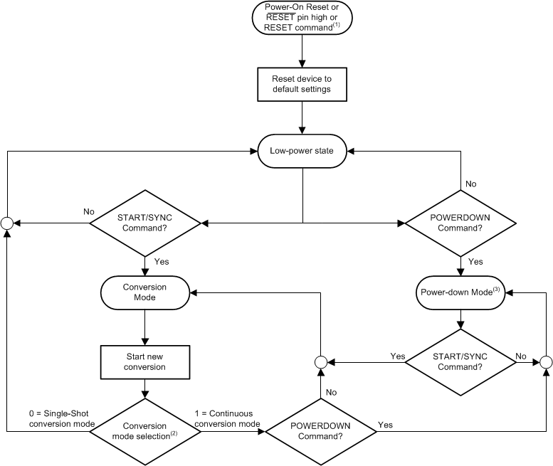
Figure 54 shows a flow chart of the different operating modes and how the device transitions from one mode to another.
ADS112C04 ai_flow_chart_sbas752.gif
Any reset (power-on, command, or pin) immediately resets the device.
The conversion mode is selected with the CM bit in the configuration register.
The POWERDOWN command allows any ongoing conversion to complete before placing the device in power-down mode.
Figure 54. Operating Flow Chart