JAJSF85A April 2018 – July 2018 OPA858
PRODUCTION DATA.
9.3.3 Wide Gain-Bandwidth Product
Figure 10 shows the open-loop magnitude and phase response of the OPA858. Calculate the gain bandwidth product of any op amp by determining the frequency at which the AOL is 60 dB and multiplying that frequency by a factor of 1000. The second pole in the AOL response occurs before the magnitude crosses 0 dB, and the resultant phase margin is less than 0°. This indicates instability at a gain of 0 dB (1 V/V). Amplifiers that are not unity-gain stable are known as decompensated amplifiers. Decompensated amplifiers typically have higher gain-bandwidth product, higher slew rate, and lower voltage noise, compared to a unity-gain stable amplifier with the same amount of quiescent power consumption.
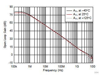
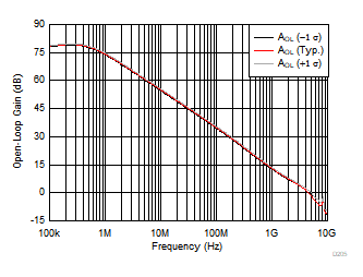
Figure 50 shows the open-loop magnitude (AOL) of the OPA858 as a function of temperature. The results show minimal variation over temperature. The phase margin of the OPA858 configured in a noise gain of 7 V/V (16.9 dB) is close to 55° across temperature. Similarly Figure 51 shows the AOL magnitude of the OPA858 as a function of process variation. The results show the AOL curve for the nominal process corner and the variation one standard deviation from the nominal. The simulated results suggest less than 1° of phase margin difference within a standard deviation of process variation when the amplifier is configured in a gain of 7 V/V.
One of the primary applications for the OPA858 is as a high-speed transimpedance amplifier (TIA), as Figure 59 shows. The low-frequency noise gain of a TIA is 0 dB (1 V/V). At high frequencies the ratio of the total input capacitance and the feedback capacitance set the noise gain. To maximize the TIA closed-loop bandwidth, the feedback capacitance is typically smaller than the input capacitance, which implies that the high-frequency noise gain is greater than 0 dB. As a result, op amps configured as TIAs are not required to be unity-gain stable, which makes a decompensated amplifier a viable option for a TIA. What You Need To Know About Transimpedance Amplifiers – Part 1 and What You Need To Know About Transimpedance Amplifiers – Part 2 describe transimpedance amplifier compensation in greater detail.
 Figure 50. Open-Loop Gain vs Temperature
  Figure 51. Open-Loop Gain vs Process Variation