JAJSF85A April   2018  – July 2018 OPA858

PRODUCTION DATA.  

  1. 特長
  2. アプリケーション
  3. 概要
    1.     Device Images
      1.      高速タイム・オブ・フライト・レシーバ
      2.      フォトダイオード容量と帯域幅およびノイズとの関係
  4. 改訂履歴
  5. Device Comparison Table
  6. Pin Configuration and Functions
    1.     Pin Functions
  7. Specifications
    1. 7.1 Absolute Maximum Ratings
    2. 7.2 ESD Ratings
    3. 7.3 Recommended Operating Conditions
    4. 7.4 Thermal Information
    5. 7.5 Electrical Characteristics
    6. 7.6 Typical Characteristics
  8. Parameter Measurement Information
    1. 8.1 Parameter Measurement Information
  9. Detailed Description
    1. 9.1 Overview
    2. 9.2 Functional Block Diagram
    3. 9.3 Feature Description
      1. 9.3.1 Input and ESD Protection
      2. 9.3.2 Feedback Pin
      3. 9.3.3 Wide Gain-Bandwidth Product
      4. 9.3.4 Slew Rate and Output Stage
      5. 9.3.5 Current Noise
    4. 9.4 Device Functional Modes
      1. 9.4.1 Split-Supply and Single-Supply Operation
      2. 9.4.2 Power-Down Mode
  10. 10Application and Implementation
    1. 10.1 Application Information
      1. 10.1.1 Using the OPA858 as a Transimpedance Amplifier
    2. 10.2 Typical Application
      1. 10.2.1 Design Requirements
      2. 10.2.2 Detailed Design Procedure
      3. 10.2.3 Application Curves
  11. 11Power Supply Recommendations
  12. 12Layout
    1. 12.1 Layout Guidelines
    2. 12.2 Layout Example
  13. 13デバイスおよびドキュメントのサポート
    1. 13.1 ドキュメントの更新通知を受け取る方法
    2. 13.2 コミュニティ・リソース
    3. 13.3 商標
    4. 13.4 静電気放電に関する注意事項
    5. 13.5 Glossary
  14. 14メカニカル、パッケージ、および注文情報

Pin Configuration and Functions

DSG Package
8-Pin WSON With Exposed Thermal Pad
Top View
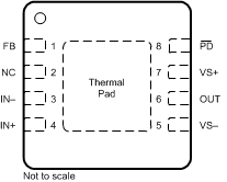
OPA858 OPA85X_DSG_pin_diagram.gif
NC - no internal connection

Pin Functions

PIN I/O DESCRIPTION
NAME NO.
FB 1 I Feedback connection to output of amplifier
IN– 3 I Inverting input
IN+ 4 I Noninverting input
NC 2 Do not connect
OUT 6 O Amplifier output
PD 8 I Power down connection. PD = logic low = power off mode; PD = logic high = normal operation
VS– 5 Negative voltage supply
VS+ 7 Positive voltage supply
Thermal pad Connect the thermal pad to VS–