JAJSFB6D April 2018 – July 2022 INA180-Q1 , INA2180-Q1 , INA4180-Q1
PRODMIX
- 1 特長
- 2 アプリケーション
- 3 概要
- 4 Revision History
- 5 Device Comparison
- 6 Pin Configuration and Functions
- 7 Specifications
- 8 Detailed Description
- 9 Application and Implementation
- 10Device and Documentation Support
8.3.4 Rail-to-Rail Output Swing
The INAx180-Q1 allow linear current sensing operation with the output close to the supply rail and GND. The maximum specified output swing to the positive rail is 30 mV, and the maximum specified output swing to GND is only 5 mV. To compare the output swing of the INAx180-Q1 to an equivalent operational amplifier (op amp), the inputs are overdriven to approximate the open-loop condition specified in op amp data sheets. The current-sense amplifier is a closed-loop system; therefore, the output swing to GND can be limited by the product of the offset voltage and amplifier gain.
For devices that have positive offset voltages, the swing to GND is limited by the larger of either the offset voltage multiplied by the gain or the swing to GND specified in the Section 7.6 table.
For example, in an application where the INA180A4-Q1 (gain = 200 V/V) is used for low-side current sensing and the device has an offset of 40 µV, the product of the device offset and gain results in a value of 8 mV, greater than the specified negative swing value. Therefore, the swing to GND for this example is 8 mV. If the same device has an offset of –40 µV, then the calculated zero differential signal is –8 mV. In this case, the offset helps overdrive the swing in the negative direction, and swing performance is consistent with the value specified in the Section 7.6 table.
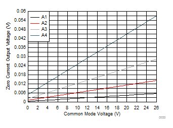
The offset voltage is a function of the common-mode voltage as determined by the CMRR specification; therefore, the offset voltage increases when higher common-mode voltages are present. The increase in offset voltage limits how low the output voltage can go during a zero-current condition when operating at higher common-mode voltages. Figure 8-5 shows the typical limitation of the zero-current output voltage vs common-mode voltage for each gain option.
 Figure 8-5 Zero-Current Output Voltage vs
Common-Mode Voltage