JAJSFI8A July   2018  – December 2018 INA253

PRODUCTION DATA.  

  1. 特長
  2. アプリケーション
  3. 概要
    1.     代表的なアプリケーション
  4. 改訂履歴
  5. Device Comparison Table
  6. Pin Configuration and Functions
    1.     Pin Functions
  7. Specifications
    1. 7.1 Absolute Maximum Ratings
    2. 7.2 ESD Ratings
    3. 7.3 Recommended Operating Conditions
    4. 7.4 Thermal Information
    5. 7.5 Electrical Characteristics
    6. 7.6 Typical Characteristics
  8. Detailed Description
    1. 8.1 Overview
    2. 8.2 Functional Block Diagram
    3. 8.3 Feature Description
      1. 8.3.1 Integrated Shunt Resistor
      2. 8.3.2 Short-Circuit Duration
      3. 8.3.3 Temperature Stability
      4. 8.3.4 Enhanced PWM Rejection Operation
      5. 8.3.5 Input Signal Bandwidth
    4. 8.4 Device Functional Modes
      1. 8.4.1 Adjusting the Output Midpoint With the Reference Pins
      2. 8.4.2 Reference Pin Connections for Unidirectional Current Measurements
      3. 8.4.3 Ground Referenced Output
      4. 8.4.4 Reference Pin Connections for Bidirectional Current Measurements
        1. 8.4.4.1 Output Set to External Reference Voltage
      5. 8.4.5 Output Set to Mid-Supply Voltage
      6. 8.4.6 Output Set to Mid-External Reference
      7. 8.4.7 Output Set Using Resistor Divide
  9. Application and Implementation
    1. 9.1 Application Information
      1. 9.1.1 Input Filtering
    2. 9.2 Typical Applications
      1. 9.2.1 High-Side, High-Drive, Solenoid Current-Sense Application
        1. 9.2.1.1 Design Requirements
        2. 9.2.1.2 Detailed Design Procedure
        3. 9.2.1.3 Application Curve
      2. 9.2.2 Speaker Enhancements and Diagnostics Using Current Sense Amplifier
        1. 9.2.2.1 Design Requirements
        2. 9.2.2.2 Detailed Design Procedure
        3. 9.2.2.3 Application Curve
      3. 9.2.3 Current Sensing for Remote I/Os in PLC
        1. 9.2.3.1 Design Requirements
        2. 9.2.3.2 Application Curve
  10. 10Power Supply Recommendations
  11. 11Layout
    1. 11.1 Layout Guidelines
    2. 11.2 Layout Example
  12. 12デバイスおよびドキュメントのサポート
    1. 12.1 デバイス・サポート
      1. 12.1.1 開発サポート
    2. 12.2 関連資料
    3. 12.3 ドキュメントの更新通知を受け取る方法
    4. 12.4 コミュニティ・リソース
    5. 12.5 商標
    6. 12.6 静電気放電に関する注意事項
    7. 12.7 Glossary
  13. 13メカニカル、パッケージ、および注文情報

Typical Characteristics

at TA = 25°C, VS = 5 V, VIN+ = 12 V, and VREF = VS / 2 (unless otherwise noted)
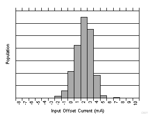
INA253 D001-SLOS954-01.gif
All gains
Figure 1. Input Offset Voltage Production Distribution
INA253 D003-SLOS954-01.gif
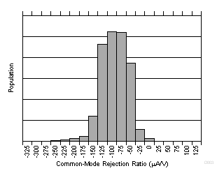
All gains
Figure 3. Common-Mode Rejection Production Distribution
INA253 D005-SLOS954-02.gif
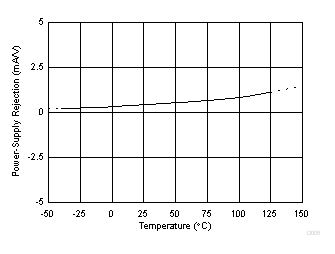
Figure 5. Power-Supply Rejection Ratio vs Temperature
INA253 D007-SLOS954-01.gif
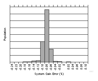
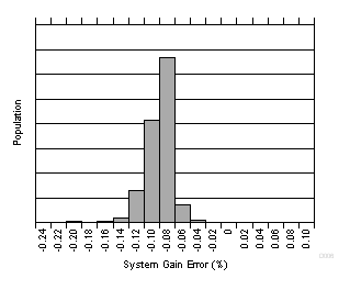
Figure 7. Gain Error Production Distribution (INA253A2)
INA253 D009-SLOS954-01.gif
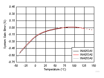
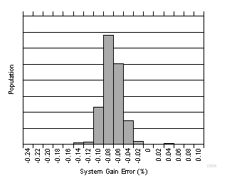
Figure 9. System Gain Error vs Temperature
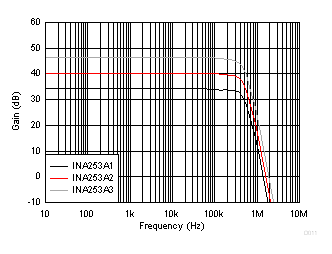
INA253 D011-SLOS954-01.gif
VCM = 0 V, VDIFF = 10-mVPP sine
Figure 11. Amplifier Gain Error vs Frequency
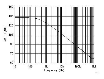
INA253 D013-SLOS954-01.gif
Figure 13. Common-Mode Rejection Ratio vs Frequency
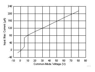
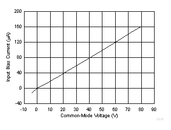
INA253 D015-SLOS954-01.gif
VS = 5 V
Figure 15. Input Bias Current vs Common-Mode Voltage
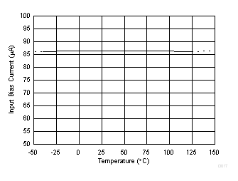
INA253 D017-SLOS954-01.gif
Figure 17. Input Bias Current vs Temperature
INA253 D019-SLOS954-01.gif
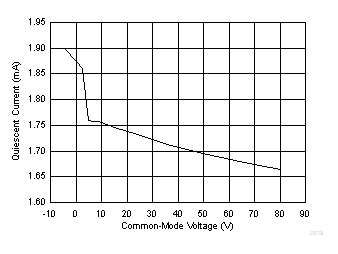
Figure 19. Quiescent Current vs Common-mode Voltage
INA253 D021-SLOS954-01.gif
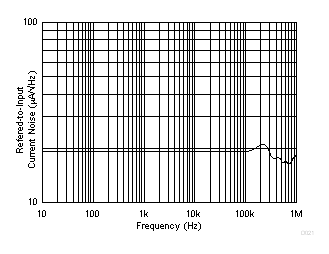
Figure 21. INA253A2 Input-Referred Voltage Noise vs Frequency
INA253 D023-SLOS954-01.gif
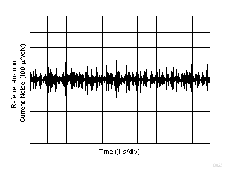
Figure 23. 0.1-Hz to 10-Hz Voltage Noise (Referred-to-Input)
INA253 D025-SLOS954-01.gif
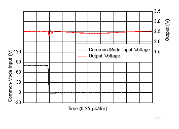
VREF1 = VREF2 = 0 V
Figure 25. Common-Mode Transient Response
INA253 D027-SLOS954-01.gif
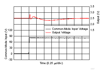
Rising Edge
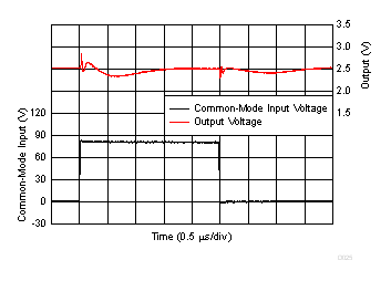
Figure 27. Common-Mode Voltage Transient Response
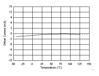
INA253 D002-SLOS954-01.gif
Figure 2. Input Offset Current vs Temperature
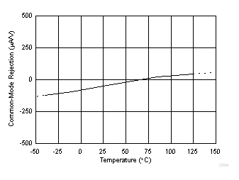
INA253 D004-SLOS954-01.gif
Figure 4. Common-Mode Rejection Ratio vs Temperature
INA253 D006-SLOS954-01.gif
Figure 6. Gain Error Production Distribution (INA253A1)
INA253 D008-SLOS954-01.gif
Figure 8. Gain Error Production Distribution (INA253A3)
INA253 D010-SLOS954-01.gif
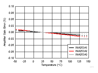
Figure 10. Amplifier Gain Error vs Temperature
INA253 D012-SLOS954-01.gif
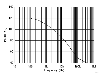
Figure 12. Power-Supply Rejection Ratio vs Frequency
INA253 D014-SLOS954-01.gif
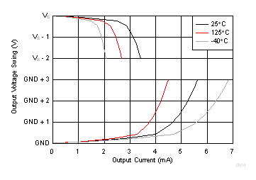
VS = 5 V
Figure 14. Output Voltage Swing vs Output Current
INA253 D016-SLOS954-01.gif
VS = 0 V
Figure 16. Input Bias Current vs Common-Mode Voltage
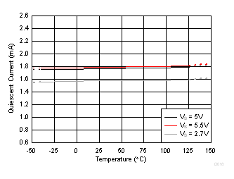
INA253 D018-SLOS954-02.gif
Figure 18. Quiescent Current vs Temperature
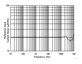
INA253 D020-SLOS954-01.gif
Figure 20. INA253A1 Input-Referred Voltage Noise vs Frequency
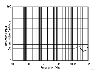
INA253 D022-SLOS954-01.gif
Figure 22. INA253A3 Input-Referred Voltage Noise vs Frequency
INA253 D024-SLOS954-01.gif
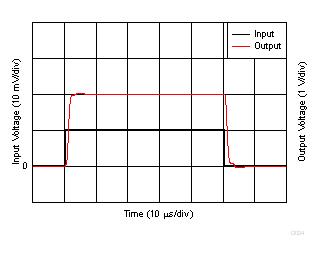
VREF1 = VREF2 = 0 V, 10-mVPP input step
Figure 24. Amplifier Step Response
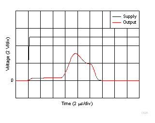
INA253 D026-SLOS954-01.gif
Figure 26. Start-Up Response
INA253 D028-SLOS954-01.gif
Falling Edge
Figure 28. Common-Mode Voltage Transient Response