JAJSFM8B June 2018 – May 2019 LMZM33606
PRODUCTION DATA.
- 1 特長
- 2 アプリケーション
- 3 概要
- 4 改訂履歴
- 5 Pin Configuration and Functions
- 6 Specifications
-
7 Detailed Description
- 7.1 Overview
- 7.2 Functional Block Diagram
- 7.3
Feature Description
- 7.3.1 Adjusting the Output Voltage
- 7.3.2 Input Capacitor Selection
- 7.3.3 Output Capacitor Selection
- 7.3.4 Transient Response
- 7.3.5 Feed-Forward Capacitor
- 7.3.6 Switching Frequency (RT)
- 7.3.7 Synchronization (SYNC/MODE)
- 7.3.8 Output Enable (EN)
- 7.3.9 Programmable System UVLO (EN)
- 7.3.10 Internal LDO and BIAS_SEL
- 7.3.11 Power Good (PGOOD) and Power Good Pull-Up (PGOOD_PU)
- 7.3.12 Mode Select (Auto or FPWM)
- 7.3.13 Soft Start and Voltage Tracking
- 7.3.14 Voltage Dropout
- 7.3.15 Overcurrent Protection (OCP)
- 7.3.16 Thermal Shutdown
- 7.4 Device Functional Modes
- 8 Application and Implementation
- 9 Power Supply Recommendations
- 10Layout
- 11デバイスおよびドキュメントのサポート
- 12メカニカル、パッケージ、および注文情報
7.3.5 Feed-Forward Capacitor
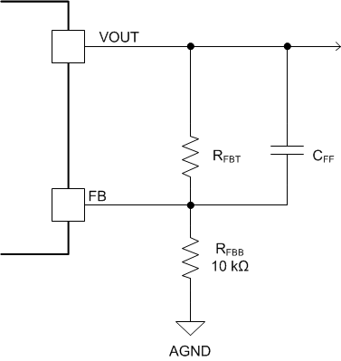
The LMZM33606 is internally compensated to be stable over the operating range of the device. However, depending on the output voltage and amount of output capacitance, a feed-forward capacitor, CFF, may be added for optimum performance. The feed-forward capacitor should be placed in parallel with the top resistor divider, RFBT as shown in Figure 32. The value for CFF can be calculated using Equation 2. For output voltages < 1.2 V, CFF is ineffective and is not recommended.
Equation 2. 

where
- COUT is in µF
- RFBT is in kΩ
 Figure 32. Feed-Forward Capacitor