JAJSFO0G
september 2012 – october 2020
SN65DSI85
PRODUCTION DATA
1
1
特長
2
アプリケーション
3
概要
4
Revision History
5
Pin Configuration and Functions
6
Specifications
6.1
Absolute Maximum Ratings #GUID-24B27461-2407-4A70-B6CA-5D1E4961612D/SLLSEB91839
6.2
ESD Ratings
6.3
Recommended Operating Conditions
6.4
Thermal Information
6.5
Electrical Characteristics
6.6
Switching Characteristics
Parameter Measurement Information
7
Detailed Description
7.1
Overview
7.2
Functional Block Diagram
7.3
Feature Description
7.3.1
Clock Configurations and Multipliers
7.3.2
ULPS
7.3.3
LVDS Pattern Generation
7.4
Device Functional Modes
7.4.1
Operating Modes
7.4.2
24
7.4.3
Reset Implementation
7.4.4
Initialization Sequence
7.4.5
LVDS Output Formats
7.4.6
DSI Lane Merging
7.4.7
DSI Pixel Stream Packets
7.4.8
DSI Video Transmission Specifications
7.5
Programming
7.5.1
Local I2C Interface Overview
7.6
Register Maps
7.6.1
Control and Status Registers Overview
8
Application and Implementation
8.1
Application Information
8.1.1
Video STOP and Restart Sequence
8.1.2
Reverse LVDS Pin Order Option
8.1.3
IRQ Usage
8.2
Typical Applications
8.2.1
Typical WUXGA 18-bpp Application
8.2.1.1
Design Requirements
8.2.1.2
Detailed Design Procedure
8.2.1.2.1
Example Script
8.2.1.3
Application Curve
8.2.2
Typical WQXGA 24-bpp Application
8.2.2.1
Design Requirements
9
Power Supply Recommendations
9.1
VCC Power Supply
9.2
VCORE Power Supply
10
Layout
10.1
Layout Guidelines
10.1.1
Package Specific
10.1.2
Differential pairs
10.1.3
Ground
10.2
Layout Example
11
Device and Documentation Support
11.1
Receiving Notification of Documentation Updates
11.2
Community Resources
11.3
Trademarks
12
Mechanical, Packaging, and Orderable Information
Abstract
Figure 7-1
SN65DSI85 FlatLink™ Timing Definitions
A.
See the
ULPS
section of the data sheet for the ULPS entry and exit sequence.
B.
ULPS entry and exit protocol and timing requirements must be met per MIPI® DPHY specification.
Figure 7-2
ULPS Timing Definition
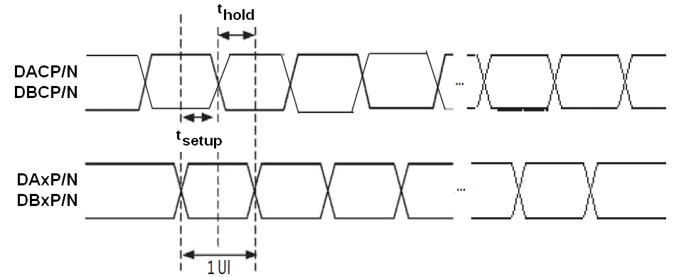
Figure 7-3
DSI HS Mode Receiver Timing Definitions