JAJSFP1G April   2016  – May 2019 DLP5531-Q1

PRODUCTION DATA.  

  1. 特長
  2. アプリケーション
  3. 概要
    1.     Device Images
      1.      DLP5531-Q1 DLPチップセットのシステム・ブロック図
  4. 改訂履歴
  5. Pin Configuration and Functions
    1.     Pin Functions – Connector Pins
    2.     Pin Functions – Test Pads
  6. Specifications
    1. 6.1  Absolute Maximum Ratings
    2. 6.2  Storage Conditions
    3. 6.3  ESD Ratings
    4. 6.4  Recommended Operating Conditions
    5. 6.5  Thermal Information
    6. 6.6  Electrical Characteristics
    7. 6.7  Timing Requirements
    8. 6.8  Switching Characteristics
    9. 6.9  System Mounting Interface Loads
    10. 6.10 Physical Characteristics of the Micromirror Array
    11. 6.11 Micromirror Array Optical Characteristics
    12. 6.12 Window Characteristics
    13. 6.13 Chipset Component Usage Specification
  7. Detailed Description
    1. 7.1 Overview
    2. 7.2 Functional Block Diagram
    3. 7.3 Feature Description
      1. 7.3.1 Sub-LVDS Data Interface
      2. 7.3.2 Low Speed Interface for Control
      3. 7.3.3 DMD Voltage Supplies
      4. 7.3.4 Asynchronous Reset
      5. 7.3.5 Temperature Sensing Diode
        1. 7.3.5.1 Temperature Sense Diode Theory
    4. 7.4 System Optical Considerations
      1. 7.4.1 Numerical Aperture and Stray Light Control
      2. 7.4.2 Pupil Match
      3. 7.4.3 Illumination Overfill
    5. 7.5 DMD Image Performance Specification
    6. 7.6 Micromirror Array Temperature Calculation
      1. 7.6.1 Temperature Rise Through the Package for Heatsink Design
      2. 7.6.2 Monitoring Array Temperature Using the Temperature Sense Diode
    7. 7.7 Micromirror Landed-On/Landed-Off Duty Cycle
      1. 7.7.1 Definition of Micromirror Landed-On/Landed-Off Duty Cycle
  8. Application and Implementation
    1. 8.1 Application Information
    2. 8.2 Typical Application
      1. 8.2.1 Application Overview
      2. 8.2.2 Reference Design
      3. 8.2.3 Application Mission Profile Consideration
  9. Power Supply Recommendations
    1. 9.1 Power Supply Power-Up Procedure
    2. 9.2 Power Supply Power-Down Procedure
    3. 9.3 Power Supply Sequencing Requirements
  10. 10Layout
    1. 10.1 Layout Guidelines
  11. 11デバイスおよびドキュメントのサポート
    1. 11.1 デバイス・サポート
      1. 11.1.1 デバイスの項目表記
      2. 11.1.2 デバイスのマーキング
    2. 11.2 関連リンク
    3. 11.3 コミュニティ・リソース
    4. 11.4 商標
    5. 11.5 静電気放電に関する注意事項
    6. 11.6 DMD の取り扱い
    7. 11.7 Glossary
  12. 12メカニカル、パッケージ、および注文情報

Temperature Sensing Diode

The DMD includes a temperature sensing diode designed to be used with the TMP411 temperature monitoring device. The DLPC230-Q1 monitors the DMD array temperature via the TMP411 and temperature sense diode. The DLPC230-Q1 operation of the DMD timing is based in part on the DMD array temperature, therefore this connection is essential to ensure reliable operation of the DMD.

Figure 16 shows the typical connection between the DLPC230-Q1, TMP411, and the DMD.
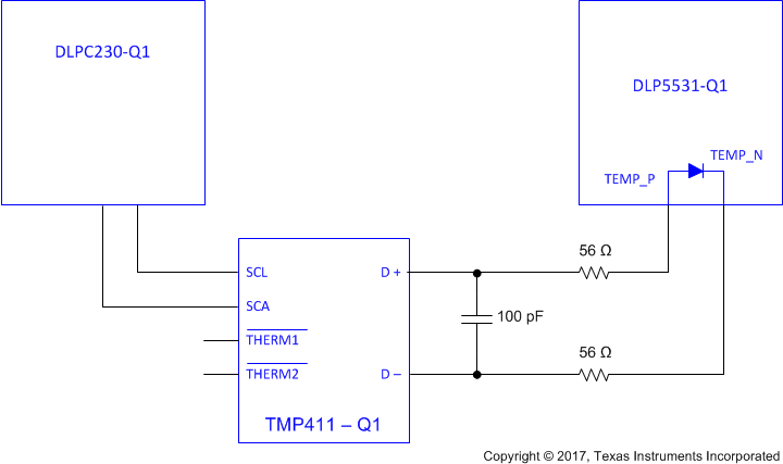
DLP5531-Q1 sec_7_temp_sense_diode.gifFigure 16. Temperature Sense Diode Typical Circuit Configuration