JAJSFP3A July 2018 – August 2018 TLC6C5716-Q1
PRODUCTION DATA.
- 1 特長
- 2 アプリケーション
- 3 概要
- 4 改訂履歴
- 5 Pin Configuration and Functions
- 6 Specifications
-
7 Detailed Description
- 7.1 Overview
- 7.2 Functional Block Diagram
- 7.3
Feature Description
- 7.3.1 Maximum Constant-Sink-Current Setting
- 7.3.2 Brightness Control and Dot Correction
- 7.3.3 Grayscale Configuration
- 7.3.4
Diagnostics
- 7.3.4.1 LED Diagnostics
- 7.3.4.2 Adjacent-Pin-Short Check
- 7.3.4.3 IREF-Short and IREF-Open Detection
- 7.3.4.4 Pre-Thermal Warning Flag
- 7.3.4.5 Thermal Error Flag
- 7.3.4.6 Negate-Bit Toggle
- 7.3.4.7 LOD_LSD Self-Test
- 7.3.4.8 ERR Pin
- 7.3.4.9 ERROR Clear
- 7.3.4.10 Global Reset
- 7.3.4.11 Slew Rate Control
- 7.3.4.12 Channel Group Delay
- 7.4 Device Functional Modes
- 7.5 Programming
- 7.6 Register Maps
- 8 Application and Implementation
- 9 Power Supply Recommendations
- 10Layout
- 11デバイスおよびドキュメントのサポート
- 12メカニカル、パッケージ、および注文情報
8.2 Typical Application
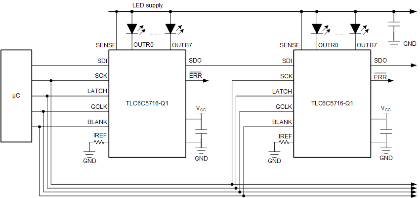
In automotive LCD display applications such as a solid-state cluster or center information display, LED backlighting is one of the key parts of the display. Today most LED backlighting is the traditional edge-lit type, which means the backlighting is globally dimmed. This method consumes much power and causes light leakage from the liquid crystals in the black areas, because the backlighting is always turned on. Recently, local-dimming backlighting, a direct-lit type of backlighting, has been proposed to overcome this drawback. The lighting level of the backlighting follows the display contents. The lighting level is dynamically adjusted by the content of the image blocks for local-dimming control. When an image block is bright, the lighting level of the backlighting turns high also. Conversely, the backlighting level is adjusted to low in a black region. This arrangement reduces power dissipation and light leakage from the LCD and creates pure black, increasing the image contrast ratio.
Users can use the TLC6C5716-Q1 device to drive LED backlighting in such local dimming applications. Depending how many zones are in the display, users can connect different numbers of TLC6C5716-Q1s in a daisy chain to drive the LEDs.
 Figure 31. Typical Block Diagram for Local Dimming