JAJSFS8B July   2018  – February 2022 BQ25601D

PRODUCTION DATA  

  1. 特長
  2. アプリケーション
  3. 説明
  4. Revision History
  5. 概要 (続き)
  6. Device Comparison Table
  7. Pin Configuration and Functions
  8. Specifications
    1. 8.1 Absolute Maximum Ratings
    2. 8.2 ESD Ratings
    3. 8.3 Recommended Operating Conditions
    4. 8.4 Thermal information
    5. 8.5 Electrical Characteristics
    6. 8.6 Timing Requirements
    7. 8.7 Typical Characteristics
  9. Detailed Description
    1. 9.1 Overview
    2. 9.2 Functional Block Diagram
    3. 9.3 Feature Description
      1. 9.3.1 Power-On-Reset (POR)
      2. 9.3.2 Device Power Up from Battery without Input Source
      3. 9.3.3 Power Up from Input Source
        1. 9.3.3.1 Power Up REGN Regulation
        2. 9.3.3.2 Poor Source Qualification
        3. 9.3.3.3 Input Source Type Detection
          1. 9.3.3.3.1 D+/D– Detection Sets Input Current Limit in BQ25601D
        4. 9.3.3.4 Input Voltage Limit Threshold Setting (VINDPM Threshold)
        5. 9.3.3.5 Converter Power-Up
      4. 9.3.4 Boost Mode Operation From Battery
      5. 9.3.5 Host Mode and Standalone Power Management
        1. 9.3.5.1 Host Mode and Default Mode in BQ25601D
      6. 9.3.6 Power Path Management
      7. 9.3.7 Battery Charging Management
        1. 9.3.7.1 Autonomous Charging Cycle
        2. 9.3.7.2 Battery Charging Profile
        3. 9.3.7.3 Charging Termination
        4. 9.3.7.4 Thermistor Qualification
        5. 9.3.7.5 JEITA Guideline Compliance During Charging Mode
        6. 9.3.7.6 Boost Mode Thermistor Monitor During Battery Discharge Mode
        7. 9.3.7.7 Charging Safety Timer
    4. 9.4 Device Functional Modes
      1. 9.4.1 Narrow VDC Architecture
      2. 9.4.2 Dynamic Power Management
      3. 9.4.3 Supplement Mode
      4. 9.4.4 Shipping Mode and QON Pin
        1. 9.4.4.1 BATFET Disable Mode (Shipping Mode)
        2. 9.4.4.2 BATFET Enable (Exit Shipping Mode)
        3. 9.4.4.3 BATFET Full System Reset
        4. 9.4.4.4 QON Pin Operations
      5. 9.4.5 Status Outputs ( PG, STAT, INT )
        1. 9.4.5.1 Power Good Indicator ( PGPin PG_STAT Bit)
        2. 9.4.5.2 Charging Status indicator (STAT)
        3. 9.4.5.3 Interrupt to Host ( INT)
    5. 9.5 Protections
      1. 9.5.1 Voltage and Current Monitoring in Converter Operation
        1. 9.5.1.1 Voltage and Current Monitoring in Buck Mode
          1. 9.5.1.1.1 Input Overvoltage (ACOV)
          2. 9.5.1.1.2 System Overvoltage Protection (SYSOVP)
      2. 9.5.2 Voltage and Current Monitoring in Boost Mode
        1. 9.5.2.1 VBUS Soft Start
        2. 9.5.2.2 VBUS Output Protection
        3. 9.5.2.3 Boost Mode Overvoltage Protection
      3. 9.5.3 Thermal Regulation and Thermal Shutdown
        1. 9.5.3.1 Thermal Protection in Buck Mode
        2. 9.5.3.2 Thermal Protection in Boost Mode
      4. 9.5.4 Battery Protection
        1. 9.5.4.1 Battery Overvoltage Protection (BATOVP)
        2. 9.5.4.2 Battery Over-Discharge Protection
        3. 9.5.4.3 System Over-Current Protection
    6. 9.6 Programming
      1. 9.6.1 Serial Interface
        1. 9.6.1.1 Data Validity
        2. 9.6.1.2 START and STOP Conditions
        3. 9.6.1.3 Byte Format
        4. 9.6.1.4 Acknowledge (ACK) and Not Acknowledge (NACK)
        5. 9.6.1.5 Slave Address and Data Direction Bit
        6. 9.6.1.6 Single Read and Write
        7. 9.6.1.7 Multi-Read and Multi-Write
    7. 9.7 Register Maps
      1. 9.7.1  REG00 (address = 00) [reset = 00010111]
      2. 9.7.2  REG01 (address = 01) [reset = 00011010]
      3. 9.7.3  REG02 (address = 02) [reset = 10100 010]
      4. 9.7.4  REG03 (address = 03) [reset = 001 0001 0]
      5. 9.7.5  REG04 (address = 04) [reset = 01011000]
      6. 9.7.6  REG05 (address = 05) [reset = 10011111]
      7. 9.7.7  REG06 (address = 06) [reset = 01100110]
      8. 9.7.8  REG07 (address = 07) [reset = 01001100]
      9. 9.7.9  REG08 (address = 08) [reset = xxxxxxxx]
      10. 9.7.10 REG09 (address = 09) [reset = xxxxxxxx]
      11. 9.7.11 REG0A (address = 0A) [reset = xxxxxx00]
      12. 9.7.12 REG0B (address = 0B) [reset = 00111xxx]
  10. 10Layout
    1. 10.1 Layout Guidelines
    2. 10.2 Layout Example
  11. 11Device and Documentation Support
    1. 11.1 Device Support
      1. 11.1.1 Third-Party Products Disclaimer
    2. 11.2 Documentation Support
      1. 11.2.1 Related Documentation
    3. 11.3 Receiving Notification of Documentation Updates
    4. 11.4 サポート・リソース
    5. 11.5 Trademarks
    6. 11.6 Electrostatic Discharge Caution
    7. 11.7 Glossary

Supplement Mode

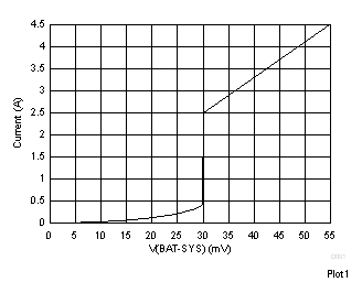
When the system voltage falls 180 mV (VBAT > VSYSMin) or 45 mV (VBAT < VSYSMin) below the battery voltage, the BATFET turns on and the BATFET gate is regulated the gate drive of BATFET so that the minimum BATFET VDS stays at 30 mV when the current is low. This prevents oscillation from entering and exiting the supplement mode.

As the discharge current increases, the BATFET gate is regulated with a higher voltage to reduce RDSON until the BATFET is in full conduction. At this point onwards, the BATFET VDS linearly increases with discharge current. Figure 9-9 shows the V-I curve of the BATFET gate regulation operation. BATFET turns off to exit supplement mode when the battery is below battery depletion threshold.
GUID-4DCFC2F7-C6F5-450C-AD1E-5A9D09C28F28-low.gifFigure 9-9 BAFET V-I Curve