JAJSFT7A
July 2018 – October 2021
TPS3431
PRODUCTION DATA
1
特長
2
アプリケーション
3
概要
4
Revision History
5
Pin Configuration and Functions
6
Specifications
6.1
Absolute Maximum Ratings
6.2
ESD Ratings
6.3
Recommended Operating Conditions
6.4
Thermal Information
6.5
Electrical Characteristics
6.6
Timing Requirements
6.7
Timing Diagrams
6.8
Typical Characteristics
7
Detailed Description
7.1
Overview
7.2
Functional Block Diagram
7.3
Feature Description
7.3.1
Enable Input (EN) and Enable Output (ENOUT)
7.3.2
Watchdog Mode
7.3.2.1
CWD
7.3.2.2
Watchdog Input WDI
7.3.2.3
Watchdog Output WDO
7.3.2.4
SET1
7.4
Device Functional Modes
7.4.1
VDD is Below VPOR ( VDD < VPOR)
7.4.2
Above Power-On-Reset, But Less Than VDD(min) (VPOR ≤ VDD < VDD(min))
7.4.3
Normal Operation (VDD ≥ VDD(min))
8
Application and Implementation
8.1
Application Information
8.1.1
CWD Functionality
8.1.1.1
Factory-Programmed Timing Options
8.1.1.2
CWD Adjustable Capacitor Watchdog Timeout
8.2
Typical Application
8.2.1
Design 1 Requirements
8.2.2
Detailed Design 1 Procedure
8.2.2.1
Calculating WDO Pullup Resistor Design 1
8.2.2.2
Setting the Watchdog Design 1
8.2.3
Application Curves Design 1
8.3
Programmable Application
8.3.1
Design 2 Requirements
8.3.2
Detailed Design 2 Procedure
8.3.2.1
Calculating WDO Pullup Resistor Design 2
8.3.2.2
Setting the Watchdog Design 2
8.3.2.3
Watchdog Disabled During Initialization Period Design 2
8.3.2.4
Programmable Disable Feature Design 2
8.3.3
Application Curves Design 2
9
Power Supply Recommendations
10
Layout
10.1
Layout Guidelines
10.2
Layout Example
11
Device and Documentation Support
11.1
Device Support
11.2
Documentation Support
11.2.1
Related Documentation
11.3
Receiving Notification of Documentation Updates
11.4
サポート・リソース
11.5
Trademarks
11.6
Electrostatic Discharge Caution
11.7
Glossary
12
Mechanical, Packaging, and Orderable Information
10.2
Layout Example
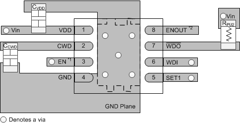
EN can also be left floating and is internally pulled-up to VDD
ENOUT can also be left floating or tied to
WDO
Figure 10-1
TPS3431
Recommended Layout